Features: •Memory storage capacity:
IDT72V3686 16,384 x 36 x 2
IDT72V3696 32,768 x 36 x 2
IDT72V36106
65,536 x 36 x 2
•Clock frequencies up to 100 MHz (6.5ns access time)
•Two independent FIFOs buffer data between one bidirectional
36-bit port and two unidirectional 18-bit ports (Port C receives
and Port B transmits)
•18-bit (word) and 9-bit (byte) bus sizing of 18 bits (word) on Ports B and C
•Select IDT Standard timing (using EFA , EFB , FFA , and FFC flag
functions) or First Word Fall Through Timing (using ORA, ORB,
IRA, and IRC flag functions)
•Programmable Almost-Empty and Almost-Full flags; each has
five default offsets (8, 16, 64, 256 and 1024)
•Serial or parallel programming of partial flags
•Big- or Little-Endian format for word and byte bus sizes
•Loopback mode on Port A
•Retransmit Capability
•Master Reset clears data and configures FIFO, Partial Reset
clears data but retains configuration settings
•Mailbox bypass registers for each FIFO
•Free-running CLKA, CLKB and CLKC may be asynchronous or
coincident (simultaneous reading and writing of data on a single
clock edge is permitted)
•Auto power down minimizes power dissipation
•Available in a space-saving 128-pin Thin Quad Flatpack (TQFP)
•Pin compatible to the lower density parts, IDT72V3626/72V3636/
72V3646/72V3656/72V3666/72V3676
•Industrial temperature range (40°C to +85°C) is availablePinout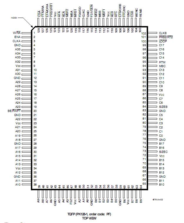 Specifications
|
Symbol |
Rating |
Commercial |
Unit |
|
VCC |
Supply Voltage Range |
0.5 to +4.6 |
V |
|
VI(2) |
Input Voltage Range |
0.5 to VCC+0.5 |
V |
|
VO(2) |
Output Voltage Range |
0.5 to VCC+0.5 |
V |
|
IIK |
Input Clamp Current (V < 0 or V > VCC) |
±20 |
mA |
|
IOK |
Output Clamp Current (VO= < 0 or VO> VCC) |
±50 |
mA |
|
IOUT |
Continuous Output Current (VO= 0 to VCC) |
±50 |
mA |
|
ICC |
Continuous Current Through VCC or GND |
±400 |
mA |
|
TSTG |
Storage Temperature Range |
65 to 150 |
°C |
DescriptionThe IDT72V36106 are designed to run off a 3.3V supply for exceptionally low-power consumption. These devices are a monolithic, high-speed, low-power, CMOS Triple Bus synchronous (clocked) FIFO memory which supports clock frequencies up to 100 MHz and has read access times as fast as 6.5ns. Two independent 16,384/32,768/65,536 x 36 dual-port SRAM FIFOs on board each chip buffer data between a bidirectional 36-bit bus (Port A) and two unidirectional 18-bit buses (Port B transmits data, Port Creceives data.) FIFO data can be read out of Port B and written into Port C using either 18-bit or 9-bit formats with a choice of Big- or Little-Endian configurations.
These devices of the IDT72V36106 are a synchronous (clocked) FIFO, meaning each port employs a synchronous interface. All data transfers through a port are gated to the LOW-to-HIGH transition of a port clock by enable signals. The clocks for each port are independent of one another and can be asynchronous orcoincident. The enables for each port are arranged to provide a simple bidirectional interface between microprocessors and/or buses with synchronous control.
Communication of the IDT72V36106 between each port may bypass the FIFOs via two mailbox registers. The mailbox registers' width matches the selected bus width of ports B and C. Each mailbox register has a flag (MBF1 and MBF2) to signal when new mail has been stored.
Two kinds of reset are available on these FIFOs of the IDT72V36106: Master Reset and Partial Reset. Master Reset initializes the read and write pointers to the first location of the memory array and selects serial flag programming, parallel flag programming, or one of five possible default flag offset settings, 8, 16, 64, 256 or 1,024.Each FIFO has its own, independent Master Reset pin,MRS1 and MRS2 .Partial Reset also sets the read and write pointers to the first location of thememory. Unlike Master Reset, any settings existing prior to Partial Reset (i.e.,programming method and partial flag default offsets) are retained. Partial Reset is useful since it permits flushing of the FIFO memory without changing any configuration settings. Each FIFO has its own, independent Partial Reset pin,PRS1 and PRS2 . Note that the Retransmit Mode, RTM pin must be LOW at the point a partial reset is performed.
Both FIFO's have Retramsmit capability, when a Retransmit is performed on a respective FIFO only the read pointer is reset to the first memory location. ARetransmit is performed by using the Retransmit Mode, RTM pin in conjunction with the Retransmit pins RT1 or RT2 , for each respective FIFO. Note that the two Retransmit pins RT1 and RT2 are muxed with the Partial Reset pins.
These devices of the IDT72V36106 have two modes of operation: In the IDT Standard mode, the first word written to an empty FIFO is deposited into the memory array. A read operation is required to access that word (along with all other words residing in memory). In the First Word Fall Through mode (FWFT), the first word written to an empty FIFO appears automatically on the outputs, no read operation required (Nevertheless, accessing subsequent words does necessitate a formal read request). The state of the BE/FWFT pin during Master Reset determines the mode in use.
Each FIFO of the IDT72V36106 has a combined Empty/Output Ready Flag (EFA /ORA and EFB/ORB) and a combined Full/Input Ready Flag (FFA/IRA and FFC/IRC). The EF and FF functions are selected in the IDT Standard mode. EF indicates whether or not the FIFO memory is empty. FF shows whether the memory is full or not. The IR and OR functions are selected in the First Word Fall Through mode. IR indicates whether or not the FIFO has available memory locations.OR shows whether the FIFO has data available for reading or not. It marks the presence of valid data on the outputs.
Each FIFO of the IDT72V36106 has a programmable Almost-Empty flag (AEA and AEB) and aprogrammable Almost-Full flag (AFA and AFC). AEA and AEB indicate when a selected number of words remain in the FIFO memory. AFA and AFC indicate when the FIFO contains more than a selected number of words.
FFA/IRA, FFC/IRC, AFA and AFC of the IDT72V36106 are two-stage synchronized to the Port Clock that writes data into its array. EFA/ORA, EFB/ORB, AEA, and AEB are two-stage synchronized to the Port Clock that reads data from its array. Programmable offsets for AEA, AEB, AFA, AFC are loaded in parallel using Port A or in serial via the SD input. Five default offset settings are also provided.The AEA and AEB threshold can be set at 8, 16, 64, 256, and 1,024 locations from the empty boundary and the AFA and AFC threshold can be set at 8, 16, 64, 256 or 1,024 locations from the full boundary. All these choices are made using the FS0, FS1 and FS2 inputs during Master Reset.
Interspersed Parity of the IDT72V36106 can also be selected during a Master Reset of the FIFO.If Interspersed Parity is selected then during parallel programming of the flag offset values, the device will ignore data line A8. If Non-Interspersed Parity is selected then data line A8 will become a valid bit.
A Loopback function of the IDT72V36106 is provided on Port A. When the Loop feature is selected via the LOOP pin, the data output from FIFO2 will be directed to the data input of FIFO1. If Loop is selected and Port A is set-up for write operation via W/RA pin, then data output from FIFO2 will be written to FIFO1, but will not be placed on the output Port A (A0-A35). If Port A is set-up for read operation via W/RA then data output from FIFO2 will be written into FIFO1 and placed onto Port A (A0-A35). The Loop will continue to happen provided that FIFO1 is not full and FIFO2 is not empty. If during a Loop sequence FIFO1 becomes full then any data that continues to be read out from FIFO2 will only be placed on the Port A (A0-A35) lines, provided that Port A is set-up for read operation. If during a Loop sequence the FIFO2 becomes empty, then the last word from FIFO2 will continue to be clocked into FIFO1 until FIFO1 becomes full or until the Loop function is stopped. The Loop feature can be useful when performing system debugging and remote loopbacks.
Two or more FIFOs of the IDT72V36106 may be used in parallel to create wider data paths. Such a width expansion requires no additional, external components. Furthermore,two IDT72V3686/72V3696/72V36106 FIFOs can be combined with unidirec-tional FIFOs capable of First Word Fall Through timing (i.e. the SuperSync FIFO family) to form a depth expansion.
If, at any time, the FIFO of the IDT72V36106 is not actively performing a function, the chip will automatically power down. During the power down state, supply current consumption (ICC) is at a minimum. Initiating any operation (by activating controlinputs) will immediately take the device out of the power down state.
The IDT72V36106 are characterized for operation from0°C to 70°C. Industrial temperature range (-40°C to +85°C) is available by special order. They are fabricated using IDT's high speed, submicron CMOS technology.

 IDT72V36106 Data Sheet