ICM7555

Features: • Exact equivalent in most applications for NE/SE555• Low supply current: 80mA (typ)• Extremely low trigger, threshold, and reset currents: 20pA (typ)• High-speed operation: 500kHz guaranteed• Wide operating supply voltage range guaranteed 3 to 16V over full...

product image

ICM7555 Picture
SeekIC No. : 004370665 Detail

ICM7555: Features: • Exact equivalent in most applications for NE/SE555• Low supply current: 80mA (typ)• Extremely low trigger, threshold, and reset currents: 20pA (typ)• High-speed o...

floor Price/Ceiling Price

Part Number:
ICM7555
Supply Ability:
5000

Price Break

  • Qty
  • 1~5000
  • Unit Price
  • Negotiable
  • Processing time
  • 15 Days
Total Cost: $ 0.00

SeekIC Buyer Protection PLUS - newly updated for 2013!

  • Escrow Protection.
  • Guaranteed refunds.
  • Secure payments.
  • Learn more >>

Month Sales

268 Transactions

Rating

evaluate  (4.8 stars)

Upload time: 2025/1/2

Payment Methods

All payment methods are secure and covered by SeekIC Buyer Protection PLUS.

Notice: When you place an order, your payment is made to SeekIC and not to your seller. SeekIC only pays the seller after confirming you have received your order. We will also never share your payment details with your seller.
Product Details

Description


Features:

• Exact equivalent in most applications for NE/SE555
• Low supply current: 80mA (typ)
• Extremely low trigger, threshold, and reset currents: 20pA (typ)
• High-speed operation: 500kHz guaranteed
• Wide operating supply voltage range guaranteed 3 to 16V over full automotive temperatures
• Normal reset function; no crowbarring of supply during output transition
• Can be used with higher-impedance timing elements than the bipolar 555 for longer time constants


Application

• Precision timing
• Pulse generation
• Sequential timing
• Time delay generation
• Pulse width modulation
• Pulse position modulation
• Missing pulse detector


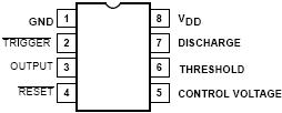
Pinout

  Connection Diagram


Specifications

SYMBOL PARAMETER RATING UNITS
VDD Supply voltage +18 V
VTRIG1
VCV
VTH
VRST
Triggerinput voltage
Control voltage
Threshold input voltage
RESETinput voltage
> -0.3 to
<VDD + 0.3
V
IOUT Output current 100 mA
PDMAX Maximum power dissipation, TA = 25°C (still air)2
N package
D package
1160
780
mW
mW
TSTG Storage temperature range -65 to +150
TSOLD Lead temperature (Soldering 60s) 300
NOTES:
1. Due to the SCR structure inherent in the CMOS process used to fabricate these devices, connecting any terminal to a voltage greater than VDD + 0.3V or less than GND -0.3V may cause destructive latch-up. For this reason it is recommended that no inputs from external sources not operating from the same power supply be applied to the device before its power supply is established. In multiple systems, the supply of the ICM7555 must be turned on first.
2. Derate above 25, at the following rates:N package at 9.3mW/ D package at 6.2mW/
3. See "Power Dissipation Considerations" section.


Description

The ICM7555 and ICM7556 are CMOS RC timers providing significantly improved performance over the standard SE/NE555/6 and 355 timers, while at the same time being direct replacements for those devices in most applications. Improved parameters include low supply current, wide operating supply voltage range, low THRESHOLD, TRIGGER and RESET currents, no crowbarring of the supply current during output transitions, higher frequency performance and no requirement to decouple CONTROL VOLTAGE for stable operation. Specifically, the ICM7555 and ICM7556 are stable controllers capable of producing accurate time delays or frequencies. The ICM7556 is a dual ICM7555, with the two timers operating independently of each other, sharing only V+ and GND. In the one shot mode, the pulse width of each circuit is precisely controlled by one external resistor and capacitor. For astable operation as an oscillator, the free running frequency and the duty cycle are both accurately controlled by two external resistors and one capacitor. Unlike the regular bipolar 555/6 devices, the CONTROL VOLTAGE terminal need not be decoupled with a capacitor. The circuits are triggered and reset on falling (negative) waveforms, and the output inverter can source or sink currents large enough to drive TTL loads, or provide minimal offsets to drive CMOS loads.


Customers Who Bought This Item Also Bought

Margin,quality,low-cost products with low minimum orders. Secure your online payments with SeekIC Buyer Protection.
Circuit Protection
Connectors, Interconnects
RF and RFID
Memory Cards, Modules
View more