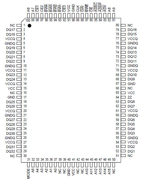
Features: • Internal self-timed write cycle• Individual Byte Write Control and Global Write• Clock controlled, registered address, data and control• Pentium™ or linear burst sequence control using MODE input• Three chip enables for simple depth expansion and add...
IC61S6432: Features: • Internal self-timed write cycle• Individual Byte Write Control and Global Write• Clock controlled, registered address, data and control• Pentium™ or linear ...
SeekIC Buyer Protection PLUS - newly updated for 2013!
268 Transactions
All payment methods are secure and covered by SeekIC Buyer Protection PLUS.
ApplicationUsing this IC socket, developers can connect a 64-pin 0.8 mm-pitch LCC (64D0) package M...
Features: • High-speed access time: 12, 15, 20, 25 ns• Low active power: 600 mW (typic...
Symbol |
Parameter |
Value |
Unit |
TBIAS |
Temperature Under Bias |
10 to +85 |
°C |
TSTG |
Storage Temperature |
55 to +150 |
°C |
PD |
Power Dissipation |
1.8 |
W |
IOUT |
Output Current (per I/O) |
100 |
mA |
VIN, VOUT |
Voltage Relative to GND for I/O Pins |
0.5 to VCCQ + 0.3 |
V |
VIN |
Voltage Relative to GND for for Address and Control Inputs |
0.5 to 5.5 |
V |
The ICSI IC61S6432 is a high-speed, low-power synchronous static RAM designed to provide a burstable, high-performance, secondary cache for the Pentium™, 680X0™, and PowerPC™ microprocessors. It is organized as 65,536 words by 32 bits, fabricated with ICSI's advanced CMOS technology. The device integrates a 2-bit burst counter, high-speed SRAM core, and high-drive capability outputs into a single monolithic circuit. All synchronous inputs pass through registers controlled by a positive-edge-triggered single clock input.
Write cycles of the IC61S6432 are internally self-timed and are initiated by the rising edge of the clock input. Write cycles can be from one to four bytes wide as controlled by the write control inputs. Separate byte enables allow individual bytes to be written.
BW1 controls DQ1-DQ8, BW2 controls DQ9-DQ16, BW3 controls DQ17-DQ24, BW4 controls DQ25-DQ32, conditioned by BWE being LOW. A LOW on GW input would cause all bytes to be written.
Bursts can be initiated with either ADSP (Address Status Processor) or ADSC (Address Status Cache Controller) input pins. Subsequent burst addresses can be generated internally by the IC61S6432 and controlled by the ADV (burst address advance) input pin.
Asynchronous signals include output enable (OE) of the IC61S6432, sleep mode input (ZZ), clock (CLK) and burst mode input (MODE).
A HIGH input on the ZZ pin puts the SRAM in the powerdown state. When ZZ is pulled LOW (or no connect), the SRAM normally operates after three cycles of the wake-up period. A LOW input, i.e., GNDQ, on MODE pin selects LINEAR Burst. A VCCQ (or no connect) on MODE pin selects INTERLEAVED Burst