Features: · 5.0 V ± 10% Read, Program, and Erase
- Minimizes system-level power requirements
· High performance
- 55 ns access time
· Compatible with JEDEC-Standard Commands
- Uses software commands, pinouts, and packages following industry standards for single power supply Flash memory
· Minimum 100,000 Program/Erase Cycles
· Sector Erase Architecture
- Eight equal size sectors of 64K bytes each
- Any combination of sectors can be erased concurrently; also supports full chip erase
· Erase Suspend/Resume
- Suspend a sector erase operation to allow a data read or programming in a sector not being erased within the same device
· Internal Erase Algorithms
- Automatically erases a sector, any combination of sectors, or the entire chip
· Internal Programming Algorithms
- Automatically programs and verifies data at a specified address.
· Low Power Consumption
- 40 mA maximum active read current
- 60 mA maximum program/erase current
- 5mA maximum standby current
· Sector Protection
- Hardware method disables any combination of sectors from a program or erase operationPinout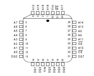 SpecificationsStorage Temperature
Plastic Package .............................. -65°C to + 125°C
Ambient Temperature
With Power Applied .......................... -55°C to + 125°C
Voltage with Respect to Ground
All pins except A9 (1) .......................... -2.0V to + 7.0V
Vcc(1) ............................................... -2.0V to + 7.0V
A9(2) ............................................... -2.0V to + 14.0V
Output Short Circuit Current(3) ......................... 200 mA
Notes:
1. Minimum DC voltage on input or I/O pins is - 0.5V. During voltage transitions, inputs may overshoot Vss to -2.0V for periods of up to 20 ns. Maximum DC voltage on output and I/O pins is Vcc + 0.5V. During Voltage transitions, outputs may overshoot to Vcc + 2.0V for periods up to 20 ns.
2. Minimum DC input voltage on A9 pin is -0.5V. During voltage transitions, A9 may overshoot Vss to -2.0V for periods of up to 20 ns. Maximum DC input voltage on A9 is + 13.5V which may overshoot to 14.0V for periods of up to 20 ns.
3. No more than one output shorted at a time. Duration of the short circuit should not be greater than one second.DescriptionThe HY29F040A is a 4 Megabit, 5.0 volt-only CMOS Flash memory device organized as a 512K bytes of 8 bits each. The device is offered in standard 32-pin PDIP, 32-pin PLCC and 32-pin TSOP packages.It is designed to be programmed and erased in-system with a 5.0 volt power-supply and can also be reprogrammed in standard PROM programmers.
The HY29F040A offers access times of 55 ns, 70 ns, 90 ns, 120 ns and 150 ns. The device has separate chip enable (/CE), write enable (/WE) and output enable (/OE) controls. Hyundai Flash memory devices reliably store memory data even after 100,000 program/erase cycles.
The HY29F040A is entirely pin and command set compatible with the JEDEC standard for 4 Megabit Flash memory devices. The commands are written to the command register using standard microprocessor write timings. Register contents serve as input to an internal state-machine which controls the erase and programming circuitry. Write cycles also internally latch addresses and data needed for the programming and erase operations.
The HY29F040A is programmed by executing the program command sequence. This will start the internal byte programming algorithm that automatically times the program pulse width and also verifies the proper cell margin. Erase is accomplished by executing either sector erase or chip erase command sequence. This will start the internal erasing algorithm that automatically times the erase pulse width and also verifies the proper cell margin. No preprogramming is required prior to execution of the internal erase algorithm. Sectors of the HY29F040A Flash memory array are electrically erased via Fowler-Nordheim tunneling. Bytes are programmed one byte at a time using a hot electron injection mechanism.
The HY29F040A features a sector erase architecture. The device memory array is divided into 8 sectors of 64K bytes each. The sectors can be erased individually or in groups without affecting the data in other sectors. The multiple sector erase and full chip erase capabilities add flexibility to altering the data in the device. To protect data in the device from accidental program and erase, the device also has a sector protect function. This function hardware write protects the selected sectors. The sector protect and sector unprotect features can be enabled in a PROM programmer.
The HY29F040A needs a single 5.0 volt powersupply for read, program and erase operation. Internally generated and well regulated voltages are provided for program and erase operation. A low Vcc detector inhibits write operations on loss of power. End of program or erase is detected by /Data Polling of DQ7 or by the Toggle Bit feature on DQ6. Once program or erase cycle is successfully completed, the device internally resets to the Read mode.

 HY29F040A Data Sheet