Collector- Emitter Voltage VCEO Max
: 600 V
Continuous Collector Current at 25 C
: 40 A
Maximum Operating Temperature
: + 150 C
Packaging
: Tube
Configuration
: Single
Maximum Gate Emitter Voltage
: +/- 20 V
Collector-Emitter Saturation Voltage
: 1.8 V
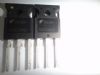
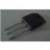
Package / Case
: TO-247-3
Gate-Emitter Leakage Current
: +/- 100 nA
Power Dissipation
: 165 W
Features: • 40A, 600V at TC = 25
• 600V Switching SOA Capability
• Typical Fall Time. . . . . . . . . . . . . . . . . . . . 140ns at 150
• Short Circuit Rated
• Low Conduction Loss
• Related Literature
- TB334 "Guidelines for Soldering Surface Mount Components to PC Boards"Pinout SpecificationsCollector to Emitter Voltage . . . . . . . . . . . . . . . . . . . . . . . . . . . . . . . . . .BVCES 600 V
Collector to Gate Voltage, RGE = 1MΩ . . . . . . . . . . . . . . . . . . . . . . . . . .BVCGR 600 V
Collector Current Continuous
At TC= 25. . . . . . . . . . . . . . . . . . . . . . . . . . . . . . . . . . . . . . . . . . . . . . . . IC25 40 A
At TC= 110. . . . . . . . . . . . . . . . . . . . . . . . . . . . . . . . . . . . . . . . . . . . . . . IC110 20A
Collector Current Pulsed (Note 1) . . . . . . . . . . . . . . . . . . . . . . . . . . . . . . . ICM 160 A
Gate to Emitter Voltage Continuous. . . . . . . . . . . . . . . . . . . . . . . . . . . . VGES ±20 V
Gate to Emitter Voltage Pulsed . . . . . . . . . . . . . . . . . . . . . . . . . . . . . . . VGEM ±30 V
Switching Safe Operating Area at TJ= 150 (Figure 2) . . . . . . . . .SSOA 30A at 600V
Power Dissipation Total at TC= 25 . . . . . . . . . . . . . . . . . . . . . . . . . . . . .. PD 165 W
Power Dissipation Derating TC> 25 . . . . . . . . . . . . . . . . . . . . . . . . . . . .. .1.32 W/
Operating and Storage Junction Temperature Range . . . . . . . . . TJ, TSTG -40 to 50
Leads at 0.063in (1.6mm) from Case for 10s. . . . . . . . . . . . . . . . . . . . . . . . .. TL300
Maximum Lead Temperature for Soldering . . . . . . . . . . . . . . . . . . . . . . . . .Tpkg 260
Short Circuit Withstand Time (Note 2) at VGE= 15V . . . . . . . . . . . . . . . . . . tSC 4µs
Short Circuit Withstand Time (Note 2) at VGE= 12V . . . . . . . . . . . . . . . . . . . tSC 10µsDescriptionThe HGT1S20N60B3S, the HGTP20N60B3 and the HGTG20N60B3 are Generation III MOS gated high voltage switching devices combining the best features of MOSFETs and bipolar transistors. These HGT1S20N60B3S, the HGTP20N60B3 and the HGTG20N60B3 have the high input impedance of a MOSFET and the low on-state conduction loss of a bipolar transistor. The much lower on-state voltage drop varies only moderately between 25 and 150.
The HGT1S20N60B3S, the HGTP20N60B3 and the HGTG20N60B3 IGBT is ideal for many high voltage switching applications operating at moderate frequencies where low conduction losses are essential, such as: AC and DC motor controls, power supplies and drivers for solenoids, relays and contactors.Formerly developmental type TA49050.
Parameters: | Technical/Catalog Information | HGTG20N60B3 |
| Vendor | Fairchild Semiconductor |
| Category | Discrete Semiconductor Products |
| Input Type | Standard |
| Voltage - Collector Emitter Breakdown (Max) | 600V |
| Current - Collector (Ic) (Max) | 40A |
| Vce(on) (Max) @ Vge, Ic | 2V @ 15V, 20A |
| Power - Max | 165W |
| Mounting Type | Through Hole |
| Package / Case | TO-247 |
| Packaging | Tube |
| Lead Free Status | Lead Free |
| RoHS Status | RoHS Compliant |
| Other Names | HGTG20N60B3
HGTG20N60B3
|

 HGTG20N60B3 Data Sheet