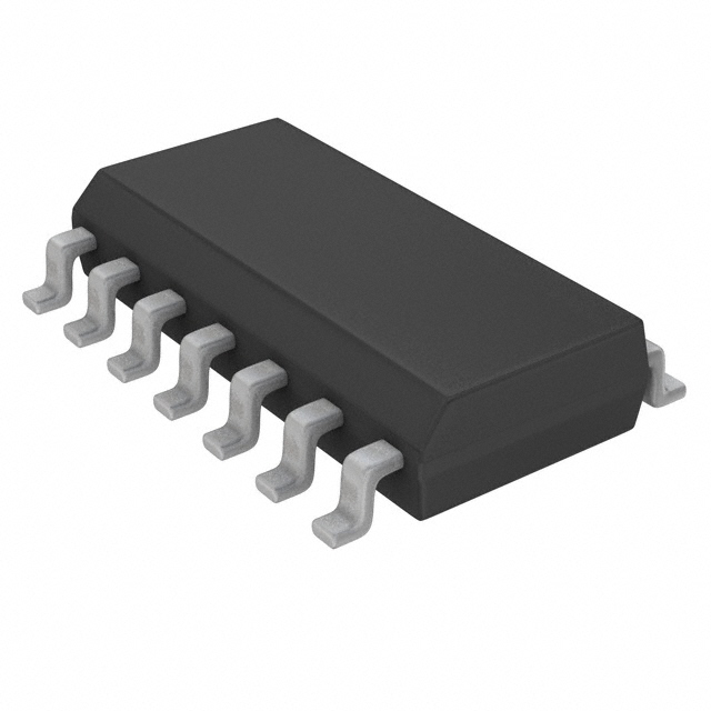
Features: ` VDD - VSS = 10V .GATED INPUTS QUIESCENT CURRENT SPECIFIED TO 20v` FOR HCC DEVICE .5V, 10V AND 15V PARAMETRIC RATINGS INPUTCURRENTOF100nA AT18VAND 25` FOR HCC DEVICE .100% TESTEDFOR QUIESCENT CURRENT MEETSALLREQUIREMENTSOFJEDECTENTATIVE STANDARD No 13 A, STANDARD SPECIFICATIONS FOR DES...
HCF4095B: Features: ` VDD - VSS = 10V .GATED INPUTS QUIESCENT CURRENT SPECIFIED TO 20v` FOR HCC DEVICE .5V, 10V AND 15V PARAMETRIC RATINGS INPUTCURRENTOF100nA AT18VAND 25` FOR HCC DEVICE .100% TESTEDFOR QUIES...
SeekIC Buyer Protection PLUS - newly updated for 2013!
268 Transactions
All payment methods are secure and covered by SeekIC Buyer Protection PLUS.
` VDD - VSS = 10V .GATED INPUTS QUIESCENT CURRENT SPECIFIED TO 20v
` FOR HCC DEVICE .5V, 10V AND 15V PARAMETRIC RATINGS INPUTCURRENTOF100nA AT18VAND 25
` FOR HCC DEVICE .100% TESTEDFOR QUIESCENT CURRENT MEETSALLREQUIREMENTSOFJEDECTENTATIVE STANDARD No 13 A, "STANDARD SPECIFICATIONS FOR DESCRIPTION OF B SERIESCMOS DEVICES"
Symbol |
Parameter |
Value |
Unit |
VDD * |
Supply Voltage: HCC Types HCF Types |
-0.5 to +20 -0.5 to +18 |
V V |
Vi |
Input Voltage |
-0.5 to VDD + 0.5 |
V |
II |
DC Input Current (any one input) |
± 10 |
mA |
Ptot |
Total Power Dissipation (per package) Dissipation per Output Transistor for Top = Full Package Temperature Range |
200 100 |
mW mW |
Top |
Operating Temperature: HCC Types HCF Types |
-55 to +125 -40 to +85 |
|
Tstg |
Storage Temperature |
-65 to +150 |
Stressesabove those listedunder "Absolute Maximum Ratings"may cause permanent damage to thedevice. This isa stress ratingonly and functional operation of the device at these or any other con ditions above those indicated in theoperational sections of this specification is not implied. Exposure to absolute maximum rating conditions for external periods may affect device reliability.
* All voltage values are referred to VSS pin voltage.
In the HCC/HCF4095B and HCC/HCF4096B series, the HCC4095B/4096B (extended temperature range) and HCF4095B/4096B (intermediate temperature range) are monolithic integrated circuits, available in 14 lead dual in-line plastic or ceramic package and plastic micropackage.
The HCC/HCF4095B and HCC/HCF4096B are J-K Master-Slave Flip-Flops featuring separate AND gating ofmultiple J and Kinputs. The gated J-Kinput control transfer of information into the master section during clocked operation. Information on the J-K inputs is transferred to the Q and Q outputs on the positive edge of the clock pulse. SET and RESET inputs (active high) are provided for asynchronous operation.