HCF4041UB

Features: · BALANCED SINK AND SOURCE CURRENT:APPROXIMATELY 4 TIMES STANDARD B DRIVE· EQUALIZED DELAY TO TRUE AND COMPLEMENT OUTPUTS· QUIESCENT CURRENT SPECIFIED UP TO 20V· STANDARDIZED SYMMETRICAL OUTPUT CHARACTERISTICS · 5V, 10V AND 15V PARAMETRIC RATINGS· INPUT LEAKAGE CURRENT II = 100nA (MAX)...

product image

HCF4041UB Picture
SeekIC No. : 004359657 Detail

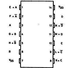
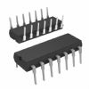
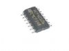
HCF4041UB: Features: · BALANCED SINK AND SOURCE CURRENT:APPROXIMATELY 4 TIMES STANDARD B DRIVE· EQUALIZED DELAY TO TRUE AND COMPLEMENT OUTPUTS· QUIESCENT CURRENT SPECIFIED UP TO 20V· STANDARDIZED SYMMETRICAL...

floor Price/Ceiling Price

Part Number:
HCF4041UB
Supply Ability:
5000

Price Break

  • Qty
  • 1~5000
  • Unit Price
  • Negotiable
  • Processing time
  • 15 Days
Total Cost: $ 0.00

SeekIC Buyer Protection PLUS - newly updated for 2013!

  • Escrow Protection.
  • Guaranteed refunds.
  • Secure payments.
  • Learn more >>

Month Sales

268 Transactions

Rating

evaluate  (4.8 stars)

Upload time: 2024/9/16

Payment Methods

All payment methods are secure and covered by SeekIC Buyer Protection PLUS.

Notice: When you place an order, your payment is made to SeekIC and not to your seller. SeekIC only pays the seller after confirming you have received your order. We will also never share your payment details with your seller.
Product Details

Description


Features:

· BALANCED SINK AND SOURCE CURRENT:APPROXIMATELY 4 TIMES STANDARD "B" DRIVE
· EQUALIZED DELAY TO TRUE AND COMPLEMENT OUTPUTS
· QUIESCENT CURRENT SPECIFIED UP TO 20V
· STANDARDIZED SYMMETRICAL OUTPUT CHARACTERISTICS
· 5V, 10V AND 15V PARAMETRIC RATINGS
· INPUT LEAKAGE CURRENT
    II = 100nA (MAX) AT VDD = 18V TA = 25°C
· 100% TESTED FOR QUIESCENT CURRENT
· MEETS ALL REQUIREMENTS OF JEDEC JESD13B " STANDARD SPECIFICATIONS FOR DESCRIPTION OF B SERIES CMOS
DEVICES"


Pinout

  Connection Diagram


Specifications

Symbol
Parameter
Value
Unit
VDD
Supply Voltage
-0.5 to +22
V
VI
DC Input Voltage
-0.5 to VDD+0.5
V
II
DC Input Current
± 10
mA
PD
Power Dissipation per Package
200
mW
Power Dissipation per Output Transistor
100
mW
TOP
Operating Temperature
-55 to +125
°C
Tstg
Storage Temperature
-65 to +150
°C

Absolute Maximum Ratings are those values beyond which damage to the device may occur. Functional operation under these conditions is not implied.
All voltage values are referred to VSS pin voltage


Description

The HCF4041UB is a monolithic integrated circuit fabricated in Metal Oxide Semiconductor technology available in DIP and SOP packages.

The HCF4041UB is a QUAD TRUE/COMPLEMENT buffer consisting of n and p channel units having low channel resistance and high current (sourcing and sinking) capability. This device is intended for use as a buffer, line driver,or CMOS to TTL driver. It can be used as an ultra-low power resistor network driver for A/D and D/A conversion, as a transmission line driver, and in other applications where high noise immunity and low power dissipation are primary design requirements.


Customers Who Bought This Item Also Bought

Margin,quality,low-cost products with low minimum orders. Secure your online payments with SeekIC Buyer Protection.
Circuit Protection
Test Equipment
Line Protection, Backups
Industrial Controls, Meters
Batteries, Chargers, Holders
View more