HCF4014B

Features: · MEDIUM SPEED OPERATION :12 MHz (Typ.) At VDD = 10V· FULLY STATIC OPERATION· 8 MASTER-SLAVE FLIP-FLOPS PLUS OUTPUT BUFFERING AND CONTROL GATING· QUIESCENT CURRENT SPECIFIED UP TO 20V· 5V, 10V AND 15V PARAMETRIC RATINGS· INPUT LEAKAGE CURRENT II= 100nA (MAX) AT VDD =18VTA = 25°C· 100% TE...

product image

HCF4014B Picture
SeekIC No. : 004359623 Detail

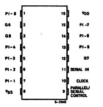
HCF4014B: Features: · MEDIUM SPEED OPERATION :12 MHz (Typ.) At VDD = 10V· FULLY STATIC OPERATION· 8 MASTER-SLAVE FLIP-FLOPS PLUS OUTPUT BUFFERING AND CONTROL GATING· QUIESCENT CURRENT SPECIFIED UP TO 20V· 5V,...

floor Price/Ceiling Price
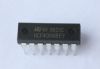
Part Number:
HCF4014B
Supply Ability:
5000

Price Break

  • Qty
  • 1~5000
  • Unit Price
  • Negotiable
  • Processing time
  • 15 Days
Total Cost: $ 0.00

SeekIC Buyer Protection PLUS - newly updated for 2013!

  • Escrow Protection.
  • Guaranteed refunds.
  • Secure payments.
  • Learn more >>

Month Sales

268 Transactions

Rating

evaluate  (4.8 stars)

Upload time: 2024/5/31

Payment Methods

All payment methods are secure and covered by SeekIC Buyer Protection PLUS.

Notice: When you place an order, your payment is made to SeekIC and not to your seller. SeekIC only pays the seller after confirming you have received your order. We will also never share your payment details with your seller.
Product Details

Description


Features:

· MEDIUM SPEED OPERATION :12 MHz (Typ.) At VDD = 10V
· FULLY STATIC OPERATION
· 8 MASTER-SLAVE FLIP-FLOPS PLUS OUTPUT BUFFERING AND CONTROL GATING
· QUIESCENT CURRENT SPECIFIED UP TO 20V
· 5V, 10V AND 15V PARAMETRIC RATINGS
· INPUT LEAKAGE CURRENT II= 100nA (MAX) AT VDD =18VTA = 25°C
· 100% TESTED FOR QUIESCENT CURRENT
· MEETS ALL REQUIREMENTS OF JEDEC JESD13B " STANDARD SPECIFICATIONS FOR DESCRIPTION OF B SERIES CMOS DEVICES"


Pinout

  Connection Diagram


Specifications

Symbol Parameter² Value Unit
VDD Supply Voltage -0.5 to +22
V
VI DC Input Voltage -0.5 to VDD + 0.5 V
II DC Input Current ± 10 mA
PD Power Dissipation per Package 200 mW
Power Dissipation per Output Transistor 100 mW
Top Operating Temperature -55 to +125
Tstg Storage Temperature -65 to +150

Absolute Maximum Ratings are those values beyond which damage to the device may occur. Functional operation under these conditions is not implied.
All voltage values are referred to VSS pin voltage.


Description

The HCF4014B is a monolithic integrated circuit fabricated in Metal Oxide Semiconductor technology available in DIP and SOP packages.

This HCF4014B is an 8-stage parallel or serial input/serial output register having common CLOCK and PARALLEL/SERIAL CONTROL inputs, a single SERIAL data input, and individual parallel "JAM"inputs to each register stage. Each register stage is a D-type, master-slave flip-flop in addition to an output from stage 8, "Q" outputs are also available from stages 6 and 7. Parallel as well as serial entry is made into the register synchronously with the positive clock line transition. In this device,entry is controlled by the PARALLEL/SERIAL CONTROL input. When the PARALLEL/SERIAL CONTROL input is low, data is serially shifted into the 8-stage register synchronously with the positive transition of he clock line. When the PARALLEL/SERIAL CONTROL input is high, data is jammed into the 8-stage register via the parallel input lines and synchronous with the positive transition of the clock line.


Customers Who Bought This Item Also Bought

Margin,quality,low-cost products with low minimum orders. Secure your online payments with SeekIC Buyer Protection.
Boxes, Enclosures, Racks
Cables, Wires
Optical Inspection Equipment
Line Protection, Backups
View more