HCF40106BE

Features: SpecificationsDescriptionThe HCF40106BE is designed as one kind of hex schmitt trigger,also it is a monolithic integrated circuit fabricated in metal oxide semiconductor technology available in DIP and SOP packages.The HCF40106BE consist of six schmitt trigger circuits each circuit funct...

product image

HCF40106BE Picture
SeekIC No. : 004359612 Detail

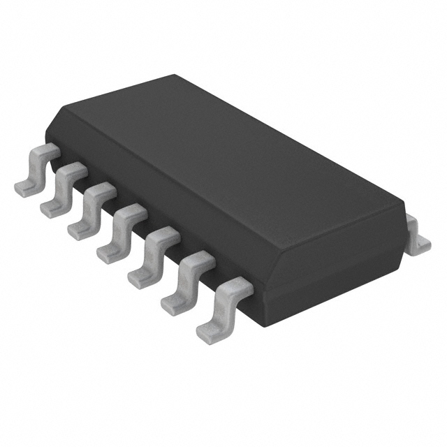
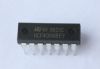
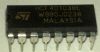
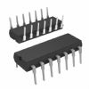
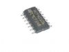
HCF40106BE: Features: SpecificationsDescriptionThe HCF40106BE is designed as one kind of hex schmitt trigger,also it is a monolithic integrated circuit fabricated in metal oxide semiconductor technology availab...

floor Price/Ceiling Price

Part Number:
HCF40106BE
Supply Ability:
5000

Price Break

  • Qty
  • 1~5000
  • Unit Price
  • Negotiable
  • Processing time
  • 15 Days
Total Cost: $ 0.00

SeekIC Buyer Protection PLUS - newly updated for 2013!

  • Escrow Protection.
  • Guaranteed refunds.
  • Secure payments.
  • Learn more >>

Month Sales

268 Transactions

Rating

evaluate  (4.8 stars)

Upload time: 2024/6/6

Payment Methods

All payment methods are secure and covered by SeekIC Buyer Protection PLUS.

Notice: When you place an order, your payment is made to SeekIC and not to your seller. SeekIC only pays the seller after confirming you have received your order. We will also never share your payment details with your seller.
Product Details

Description


Features:


Specifications


Description

The HCF40106BE is designed as one kind of hex schmitt trigger,also it is a monolithic integrated circuit fabricated in metal oxide semiconductor technology available in DIP and SOP packages.The HCF40106BE consist of six schmitt trigger circuits each circuit functions as an inverter with schmitt trigger action on the input.The trigger switches at different points for positive and negative going signals.The difference between the positive going voltage (VP) and the negative
going voltage (VN) is defined as hysteresis voltage (VH).

Features of the HCF40106BE are:(1)schmitt trigger action with no external components;(2)hysteresis voltage(typ.):0.9 V at Vdd=5 V;2.3 V at Vdd=10 V;3.5 V at Vdd=15 V;(3)noise immunity greater than 50%;(4)no limit on input rise and fall time;(5)low Vdd to Vss current during slow input ramp;(6)standardized symmetrical output characteristics;(7)quiescenr current specified up to 20 V;(8)5V,10V and 15V parametric ratings;(9)input leakage current Ii=100nA at Vdd=18V Ta=25;(10)100% tested for quiescent current.

The absolute maximum ratings of the HCF40106BE can be summarized as:(1)supply voltage:-0.5 to +22 V;(2)DC input voltage:-0.5 to VDD +0.5 V;(3)DC input current:±10 mA;(4)power dissipation per package:200 mW;(5)power dissipation per output transistor:100 mW;(6)operating temperature:-55 to +125°C;(7)storage temperature:-65 to +150°C.Absolute Maximum Ratings are those values beyond which damage to the device may occur.Functional operation under these conditions is not implied.All voltage values are referred to VSS pin voltage.


Customers Who Bought This Item Also Bought

Margin,quality,low-cost products with low minimum orders. Secure your online payments with SeekIC Buyer Protection.
RF and RFID
Resistors
Motors, Solenoids, Driver Boards/Modules
Hardware, Fasteners, Accessories
View more