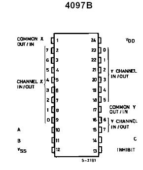
Features: `LOW ON RESISTANCE: 125W (typ.) OVER 15 Vp-p SIGNAL INPUT RANGE FOR VDD - VSS = 15V
`HIGH OFF RESISTANCE: CHANNEL LEAKAGE OF ±10pA (typ.) @ VDD - VSS = 10V
`MATCHED SWITCH CHARACTERISTICS: DRON = 5W(typ.) FOR VDD - VSS = 15V
`VERY LOW QUIESCENT POWER DISSIPATION UNDER A DIGITAL CONTROL INPUT AND SUPPLY CONDITIONS: 0.2mW (typ.) @ VDD -VSS = 10V
`BINARY ADDRESSDECODING ON CHIP
`QUIESCENT CURRENT SPECIFIED TO 20V FOR HCC DEVICE
`STANDARDIZED SYMMETRICAL OUTPUT CHARACTERISTICS
`5V, 10V AND 15V PARAMETRIC RATINGS
`INPUT CURRENT OF 100nA AT 18V AND25 FOR HCC DEVICE
`100% TESTEDFOR QUIESCENT CURRENT
`MEETSALLREQUIREMENTSOFJEDECTENTATIVE STANDARD No 13A, "STANDARD SPECIFICATIONS FOR DESCRIPTION OF B SERIE CMOS DEVICES"Pinout
Specifications
| Symbol |
Parameter |
Value |
Unit
|
| VDD* |
Supply Voltage :HCC Types
HCF Types |
0.5 to + 20
0.5 to + 18 |
V
V |
| Vi |
Input Voltage |
0.5 to VDD + 0.5 |
V |
| II |
DC Input Current (any one input) |
± 10 |
mA |
| Ptot |
Total Power Dissipation (per package)
Dissipation per Output Transistor
for Top = Full Package-temperature Range |
200
100 |
mW
mW |
| Top |
Operating Temperature : HCC Types
HCF Types |
55 to + 125
40 to + 85 |
|
| Tstg |
Storage Temperature |
65 to + 150 |
|
DescriptionIn the HCC/HCF4067B and HCC/HCF4097B series, the HCC4067B, HCC4097B (extended temperature range) and HCF4067B, HCF4097B (intermediate temperature range) are monolithic integrated circuits available in 24-lead dual in line plastic or ceramic package.
The HCC/HCF4067B and HCC/HCF4097B COS/MOS analog multiplexers/demultiplexers are digitally controlled analog switches having low ON impedance, low OFF leakage current and internal address decoding. in addition, the ON resistance is relatively constant over the full input-signal range.
The HCC/HCF4067B and HCC/HCF4097B are 16-channel multiplexer with four binary control inputs A, B, C, D, and an inhibit input, arranged so that any combination of the inputs selects one switch.
The HCC/HCF4067B and HCC/HCF4097B are differential 8-channel multiplexerhaving three binary control inputs A, B, C, and an inhibit input. The inputs permit selection of one

 HCC4097B Data Sheet


