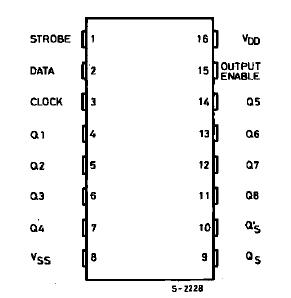
Features: .3-STATE PARALLEL OUTPUTS FOR CON- NECTIONTO COMMON BUS` SEPARATE SERIAL OUTPUTS SYNCHRONOUSTO BOTH POSITIVE AND NEGA TIVE CLOCK EDGES FOR CASCADING. MEDIUM SPEEDOPERATION 5MHz AT 10V ` STANDARDIZED SYMMETRICAL OUTPUT CHARACTERISTICS ` QUIESCENT CURRENT SPECIFIED TO 20V FOR HCC DEVICE . ...
HCC4094B: Features: .3-STATE PARALLEL OUTPUTS FOR CON- NECTIONTO COMMON BUS` SEPARATE SERIAL OUTPUTS SYNCHRONOUSTO BOTH POSITIVE AND NEGA TIVE CLOCK EDGES FOR CASCADING. MEDIUM SPEEDOPERATION 5MHz AT 10V ` ST...
SeekIC Buyer Protection PLUS - newly updated for 2013!
268 Transactions
All payment methods are secure and covered by SeekIC Buyer Protection PLUS.
Symbol | Parameter |
Value |
Unit |
VDD* | Supply Voltage : HCC Types HCF Types |
0.5 to + 20 0.5 to + 18 |
V |
Vi | Input Voltage |
0.5 to VDD + 0.5 |
A |
II | DC Input Current (any one input) |
± 10 |
mA |
Ptot | Total Power Dissipation (per package) Dissipation per Output Transistor for Top = Full Package-temperature Range |
200 100 |
mW mW |
Top | Operating Temperature : HCC Types HCF Types |
55 to + 125 40 to + 85 |
|
Tstg | Storage Temperature |
-65 to 150 |
The HCC/HCF4094B are monolithic integrated circuits available in 16-lead dual in-line plastic or ceramic packageand plastic micropackage.
The HCC/HCF4094B is an 8-stage serial shift register having a storage latch associated with each stage for strobing data from the serial input to parallel buffered 3-state outputs. The parallel outputs may be connected directly to common bus lines. Data is shifted on positive clock transitions. The data in each shift register stage is transferred to the storage register when the STROBE input is high. Data in thestorage register appears at the outputs whenever the OUTPUT-ENABLE signal is high. Two serial outputs are available for cascading a number of HCC/HCF4094B devices. Data is available at the QS serial output terminal on positive clock edges to allow for high-speed operation in cascaded systems in which the clock rise time is fast. The same serial information, available at theQ'S terminal on the next negative clock edge, provides a means for cascading HCC/HCF4094B devices when the clock rise time is slow.