Pinout Description
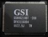
The GS881Z18BT-300 is a 9Mbit synchronous static SRAM,GSI's NBT SRAMs,like ZBT,NtRAM,NoBL or other pipelined read/double late write or flow through read/single late wire SRAMs,allow utilization of all available bus bandwidth by eliminating the need to insert deselect cycles when the GS881Z18BT-300 is switched from read to write cycles.
Features of the GS881Z18BT-300 are:(1)user-configurable pipeline and flow through mode;(2)NBT functionality allows zero wait read-write-read bus utilization;(3)fully pin-compatible with both pipelined and flow through NtRAM,NoBL and ZBT SRAMs;(4)IEEE 1149;(5)on-chip write parity checking;ever or odd selectable;(6)2.5V or 3.3V +10%/-10% core power supply;(7)2.5V or 3.3V I/O supply;(8)LBO pin for linear or interleave burst mode;(9)pin-compatible with 2M,4M,and 18M devices;(10)byte write operation (9-bit bytes);(11)3 chip enable signals for easy depth expansion;(12)ZZ pin for automatic power-down;(13)JEDEC-standard package;(14)pb-free 100-lead TQFP package available.
The absolute maximum ratings of the GS881Z18BT-300 can be summarized as:(1):the symbol is VDD,the description is voltage on VDD pins,the value is -0.5 to 4.6,the unit V;(2):the symbol is VDDQ,the description is voltage on VDDQ pins,the value is -0.5 to 4.6,the unit V;(3):the symbol is VI/O,the description is voltage on I/O pins,the value is -0.5 to VDDQ+0.5,the unit V;(4):the symbol is VIN,the description is voltage on other input pins,the value is -0.5 to VDDQ+0.5,the unit V;(5):the symbol is IIN,the description is input current on any I/O pin,the value is +/-20,the unit mA;(6):the symbol is IOUT,the description is output current on any I/O pin,the value is +/-20,the unit mA;(7):the symbol is Pd,the description is package power dissipation,the value is 1.5,the unit W;(8):the symbol is TSTG,the description is storage temperature,the value is -55 to 125,the unit ;(9):the symbol is TBIAS,the description is temperature under bias,the value is -55 to 125,the unit .

 GS881Z18BT-300 Data Sheet