GS8161E18D-200

Features: • FT pin for user-configurable flow through or pipeline operation• Dual Cycle Deselect (DCD) operation• IEEE 1149.1 JTAG-compatible Boundary Scan• 2.5 V or 3.3 V +10%/10% core power supply• 2.5 V or 3.3 V I/O supply• LBO pin for Linear or Interleaved B...

product image

GS8161E18D-200 Picture
SeekIC No. : 004355824 Detail

GS8161E18D-200: Features: • FT pin for user-configurable flow through or pipeline operation• Dual Cycle Deselect (DCD) operation• IEEE 1149.1 JTAG-compatible Boundary Scan• 2.5 V or 3.3 V +1...

floor Price/Ceiling Price

Part Number:
GS8161E18D-200
Supply Ability:
5000

Price Break

  • Qty
  • 1~5000
  • Unit Price
  • Negotiable
  • Processing time
  • 15 Days
Total Cost: $ 0.00

SeekIC Buyer Protection PLUS - newly updated for 2013!

  • Escrow Protection.
  • Guaranteed refunds.
  • Secure payments.
  • Learn more >>

Month Sales

268 Transactions

Rating

evaluate  (4.8 stars)

Upload time: 2024/12/21

Payment Methods

All payment methods are secure and covered by SeekIC Buyer Protection PLUS.

Notice: When you place an order, your payment is made to SeekIC and not to your seller. SeekIC only pays the seller after confirming you have received your order. We will also never share your payment details with your seller.
Product Details

Description


Features:

FT pin for user-configurable flow through or pipeline operation
• Dual Cycle Deselect (DCD) operation
IEEE 1149.1 JTAG-compatible Boundary Scan
• 2.5 V or 3.3 V +10%/10% core power supply
• 2.5 V or 3.3 V I/O supply
LBO pin for Linear or Interleaved Burst mode
• Internal input resistors on mode pins allow floating mode pins
• Default to Interleaved Pipeline mode
• Byte Write (BW) and/or Global Write (GW) operation
• Internal self-timed write cycle
• Automatic power-down for portable applications
• JEDEC-standard 100-lead TQFP and 165-bump BGA packages


Application

The GS8161E18(T/D)/GS8161E32(D)/GS8161E36(T/D) is a 18,874,368-bit high performance synchronous SRAM with a 2-bit burst address counter. Although of a type originally developed for Level 2 Cache applications supporting high performance CPUs, the device now finds application in synchronous SRAM applications, ranging from DSP main store to networking chip set support.


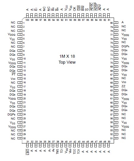
Pinout

  Connection Diagram


Specifications

Symbol

Description

Value

Unit

VDD

Voltage on VDD Pins

0.5 to 4.6

V

VDDQ

Voltage in VDDQ Pins

0.5 to 4.6

V

VI/O

Voltage on I/O Pins

0.5 to VDDQ +0.5 ( 4.6 V max.)

V

VIN

Voltage on Other Input Pins

0.5 to VDD +0.5 ( 4.6 V max.)

V

IIN

Input Current on Any Pin

+/20

mA

IOUT

Output Current on Any I/O Pin

+/20

mA

PD

Package Power Dissipation

1.5

W

TSTG

Storage Temperature

55 to 125

oC

TBIAS

Temperature Under Bias

55 to 125

oC


Customers Who Bought This Item Also Bought

Margin,quality,low-cost products with low minimum orders. Secure your online payments with SeekIC Buyer Protection.
Line Protection, Backups
Programmers, Development Systems
Motors, Solenoids, Driver Boards/Modules
Batteries, Chargers, Holders
Integrated Circuits (ICs)
Tapes, Adhesives
803
View more