EN25F40

Features: • Single power supply operation- Full voltage range: 2.7-3.6 volt• 4 Mbit Serial Flash- 4 M-bit/512 K-byte/2048 pages- 256 bytes per programmable page• High performance- 100MHz clock rate• Low power consumption- 5 mA typical active current- 1 A typical power down ...

product image

EN25F40 Picture
SeekIC No. : 004336561 Detail

EN25F40: Features: • Single power supply operation- Full voltage range: 2.7-3.6 volt• 4 Mbit Serial Flash- 4 M-bit/512 K-byte/2048 pages- 256 bytes per programmable page• High performance- ...

floor Price/Ceiling Price

Part Number:
EN25F40
Supply Ability:
5000

Price Break

  • Qty
  • 1~5000
  • Unit Price
  • Negotiable
  • Processing time
  • 15 Days
Total Cost: $ 0.00

SeekIC Buyer Protection PLUS - newly updated for 2013!

  • Escrow Protection.
  • Guaranteed refunds.
  • Secure payments.
  • Learn more >>

Month Sales

268 Transactions

Rating

evaluate  (4.8 stars)

Upload time: 2024/11/23

Payment Methods

All payment methods are secure and covered by SeekIC Buyer Protection PLUS.

Notice: When you place an order, your payment is made to SeekIC and not to your seller. SeekIC only pays the seller after confirming you have received your order. We will also never share your payment details with your seller.
Product Details

Description


Features:

• Single power supply operation
- Full voltage range: 2.7-3.6 volt
• 4 Mbit Serial Flash
- 4 M-bit/512 K-byte/2048 pages
- 256 bytes per programmable page
• High performance
- 100MHz clock rate
• Low power consumption
- 5 mA typical active current
- 1 A typical power down current
• Uniform Sector Architecture:
- 128 sectors of 4-Kbyte
- 8 blocks of 64-Kbyte
- Any sector or block can be erased individually
• Software and Hardware Write Protection:
- Write Protect all or portion of memory via software
- Enable/Disable protection with WP# pin
• High performance program/erase speed
- Page program time: 1.5ms typical
- Sector erase time: 150ms typical
- Block erase time 800ms typical
- Chip erase time: 5 Seconds typical
• Lockable 256 byte OTP security sector
• Minimum 100K endurance cycle
• Package Options
- 8 pins SOP 150mil body width
- 8 pins SOP 200mil body width
- 8 contact VDFN
- 8 pins PDIP
- All Pb-free packages are RoHS compliant
• Commercial and industrial temperature Range


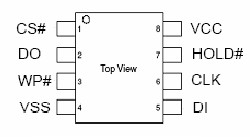
Pinout

  Connection Diagram


Specifications

Parameter Value Unit
Storage Temperature -65 to +125 °C
Plastic Packages -65 to +125 °C
Output Short Circuit Current1 200 mA
Input and Output Voltage (with respect to ground) 2 -0.5 to +4.0 V
Vcc -0.5 to +4.0 V

Notes:
1. No more than one output shorted at a time. Duration of the short circuit should not be greater than one second.
2. Minimum DC voltage on input or I/O pins is 0.5 V. During voltage transitions, inputs may undershoot Vss to 1.0V for periods of up to 50ns and to 2.0 V for periods of up to 20ns. See figure below. Maximum DC voltage on output and I/O pins is Vcc + 0.5 V. During voltage transitions, outputs may overshoot to Vcc + 1.5 V for periods up to 20ns. See figure below.


Description

The EN25F40 is a 4M-bit (512K-byte) Serial Flash memory, with advanced write protection mechanisms, accessed by a high speed SPI-compatible bus. The memory can be programmed 1 to 256 bytes at a time, using the Page Program instruction. The EN25F40 is designed to allow either single Sector at a time or full chip erase operation.

The EN25F40 can be configured to protect part of the memory as the software protected mode. The device can sustain a minimum of 100K program/erase cycles on each sector.


Customers Who Bought This Item Also Bought

Margin,quality,low-cost products with low minimum orders. Secure your online payments with SeekIC Buyer Protection.
Cables, Wires
Audio Products
Cable Assemblies
Prototyping Products
DE1
Semiconductor Modules
Computers, Office - Components, Accessories
View more