EDD5104ABTA

Features: 2.5 V power supply: VDDQ = 2.5V ± 0.2V : VDD = 2.5V ± 0.2V Data Rate: 333Mbps/266Mbps (max.) Double Data Rate architecture; two data transfers pe clock cycle Bi-directional, data strobe (DQS) is transmitted /received with data, to be used in capturing data at the receiver Data inputs, o...

product image

EDD5104ABTA Picture
SeekIC No. : 004333771 Detail

EDD5104ABTA: Features: 2.5 V power supply: VDDQ = 2.5V ± 0.2V : VDD = 2.5V ± 0.2V Data Rate: 333Mbps/266Mbps (max.) Double Data Rate architecture; two data transfers pe clock cycle Bi-directional, data strobe (...

floor Price/Ceiling Price

Part Number:
EDD5104ABTA
Supply Ability:
5000

Price Break

  • Qty
  • 1~5000
  • Unit Price
  • Negotiable
  • Processing time
  • 15 Days
Total Cost: $ 0.00

SeekIC Buyer Protection PLUS - newly updated for 2013!

  • Escrow Protection.
  • Guaranteed refunds.
  • Secure payments.
  • Learn more >>

Month Sales

268 Transactions

Rating

evaluate  (4.8 stars)

Upload time: 2024/12/25

Payment Methods

All payment methods are secure and covered by SeekIC Buyer Protection PLUS.

Notice: When you place an order, your payment is made to SeekIC and not to your seller. SeekIC only pays the seller after confirming you have received your order. We will also never share your payment details with your seller.
Product Details

Description


Features:

2.5 V power supply:  VDDQ = 2.5V ± 0.2V
                                 :  VDD = 2.5V ± 0.2V
Data Rate: 333Mbps/266Mbps (max.)
Double Data Rate architecture; two data transfers pe clock cycle 
Bi-directional, data strobe (DQS) is transmitted /received with data, to be used in capturing data at the receiver 
Data inputs, outputs, and DM are synchronized with DQS
4 internal banks for concurrent operation
DQS is edge aligned with data for READs; center aligned with data for WRITEs
Differential clock inputs (CK and /CK)
DLL aligns DQ and DQS transitions with CK transitions
Commands entered on each positive CK edge; data and data mask referenced to both edges of DQS
Data mask (DM) for write data
Auto precharge option for each burst access
2.5 V (SSTL_2 compatible) I/O
Programmable burst length (BL):  2, 4, 8
Programmable /CAS latency (CL): 2, 2.5
Refresh cycles:  8192 refresh cycles/64ms
   -7.8s maximum average periodic refresh interval
2 variations of refresh 
   -Auto refresh 
   -Self refresh 


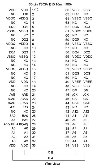
Pinout

  Connection Diagram


Specifications

Parameter Symbol Rating Unit Note
Voltage on any pin relative to VSS VT -1.0 to +3.6 V  
Supply voltage relative to VSS VDD -1.0 to +3.6 V  
Short circuit output current IOS 50 mA  
Power dissipation PD 1.0 W  
Operating ambient temperature TA 0 to +70 °C  
Storage temperature Tstg -55 to +125 °C  


Description

The EDD5104AB is a 512M bits Double Data Rate (DDR) SDRAM organized as 33,554,432 words × 4 bits × 4 banks.  The EDD5108AB is a 512M bits DDR SDRAM organized as 16,777,216 words × 8 bits × 4 banks.  Read and write operations are performed at the cross points of the CK and the /CK. This high-speed data transfer EDD5104AB is realized by the 2 bits prefetch-pipelined
architecture.  Data strobe (DQS) both for read and write are available for high speed and reliable data bus design. By setting extended mode resistor, the on-chip Delay Locked Loop (DLL) can be set enable or disable. They are packaged in standard 66-pin plastic TSOP (II)10.16mm(400).


Customers Who Bought This Item Also Bought

Margin,quality,low-cost products with low minimum orders. Secure your online payments with SeekIC Buyer Protection.
Programmers, Development Systems
Memory Cards, Modules
RF and RFID
Isolators
Semiconductor Modules
View more