Features: • Ideal for EISA bus PCs
• Functionally compatible with MC146818 in 32 KHz mode
• Totally nonvolatile with over 10 years of operation in the absence of power
• Self-contained subsystem includes lithium, quartz, and support circuitry
• Counts seconds, minutes, hours, day of the week, date, month, and year with leap year compensation
• Binary or BCD representations of time, calendar, and alarm
• 12- or 24-hour clock with AM and PM in 12-hour mode
• Daylight Savings Time option
• Interfaced with software as 64 register/RAM locations plus 8K x 8 of static RAM
14 bytes of clock and control registers
50 bytes of general and control registers
Separate 8K x 8 nonvolatile SRAM
• Programmable square wave output signal
• Bus-compatible interrupt signals (IRQ)
• Three interrupts are separately software-maskable and testable:
Time-of-day alarm once/second to once/day
Periodic rates from 122 ms to 500 ms
End-of-clock update cycle
• 28-pin JEDEC footprint
• Available as chip (DS1495/DS1495S) or stand alone module with embedded lithium battery and crystal (DS1497)
Pinout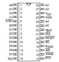 Specifications
VDD Pin Potential to Ground Pin ..............................-0.3V to +7.0V
Input Voltage ............................................VSS 0.3 to VDD + 0.3V
Power Dissipation ..............................................................500 mW
Storage Temperature DS1497:................................ 40 to +70
DS1495: .................................................................55 to +125
Ambient Temperature .....................................................0 to 70
Soldering Temperature ....................................260 for 10 seconds
* This is a stress rating only and functional operation of the device at these or any other conditions above those
indicated in the operation sections of this specification is not implied. Exposure to absolute maximum rating conditions for extended periods of time may affect reliability.
DescriptionVDD, VSS Bus operational power is supplied to the part via these pins. The voltage level present on these pins should be monitored to transition between operational power and battery power.
D0-D7 Data Bus (bidirectional): Data is written into the device from the data bus if either XRAM or RTC is asserted during a write cycle at the rising edge of a WR pulse. Data is read from the device and driven onto the data bus if either XRAM or RTC is asserted during a read cycle when the RD signal is low.
DS1495 A0-A5 Address Bus (input): Various internal registers of the device are selected by these lines. When RTC is asserted, A0 selects between the indirect address register and RTC data register. When the XRAM is asserted, A0-A5 addresses a 32byte page of RAM.
When DS1495 A5 is high, the RAM page register is accessible.
When DS1495 A5 is low, A0-A4 address the 32-byte page of RAM.
DS1495 RD Read Strobe (input): Data is read from the selected register and driven onto the data bus by the device when this line is low and either RTC or XRAM is asserted.
DS1495 WR Write Strobe (input): Data is written into the device from the data bus on the rising edge after a low pulse on this line when the device has been selected by either the XRAM or RTC signals.
DS1495 STBY Standby (input): Accesses to the device are inhibited and outputs are tri-stated to a high impedance state when this signal is asserted low. All data in RAM of the device is preserved. The real time clock continues to keep time.
If a read or write cycle is in progress when the STBY signal is asserted low, the internal cycle will be terminated when either the external cycle completes or when the internal chip enable condition (VDD is 4.25 volts, typical) is negated, whichever occurs first.
DS1495 RTC Real Time Clock Select (input): When this signal is asserted low, the real time clock registers are accessible.
Registers are selected by the A0 line. Data is driven onto the data bus when RD is low. Data is received from the bus when WR is pulsed low and then high.
DS1495 SQW Square Wave (output): Frequency selectable output. Frequency is selected by setting register A bits RSO-RS3. See Table 2 for frequencies that can be selected.
DS1495 XRAM Extended RAM Select (input): When this signal is asserted low, the extended RAM bytes are accessible.
The DS1495 XRAM page register is selected when the A5 address line is high. A 32-byte page of RAM is accessible when A5 is low. A0-A4 select the bytes within the page of RAM pointed to by the page register. Data is driven onto the data bus when RD is low. Data is received from the bus when WR is pulsed low and then high.
DS1495 IRQ Interrupt Request (output): The IRQ signal is an active low, open drain output that is used as a processor interrupt request. The IRQ output follows the state of the IRQF bit (bit 7) in status register C. IRQ can be asserted by the alarm, update ended, or periodic interrupt functions depending on the configuration of register B.
DS1495 RESET Reset (input): The reset signal is used to initialize certain registers to allow proper operation of the RTC module. When RESET is low, the following occurs.
1. The following DS1495 register bits are cleared:
a. Periodic interrupt (PIE)
b. Alarm interrupt enable (AIE)
c. Update ended interrupt (UF)
d. Interrupt request flag (IRQF)
e. Periodic interrupt flag (PF)
f. Alarm interrupt flag (AF)
g. Square wave output enable (SQWE)
h. Update ended interrupt enable (UIE)
2. The IRQ pin is in the high impedance state.
3. The RTC is not processor accessible.

 DS1495 Data Sheet


