Features: ·Operates at 2-bit Non-Return to Zero (NRZ) Data Rates up to 50 Mbits/second
· Single a5V Power Supply Operation
· Low Power Dissipation when TTL compatible code output is selected. 150 mW at 50 Mbits/second NRZ Rate
·TTL Compatible Inputs and Outputs
· ECL Compatible Code Outputs (patented) are control register selectable
· Two-bit NRZ Interface
· Supports Write Data Precompensation with Early and Late output signals
· Selectable use of either an Internal or External Write Clock
· Power Down Mode Included
· DC-Erasure is available to support Analog Flaw Mapping Testing
· Bypass Mode available which permits Un-Encoded Test Patterns to be issued at the CODEOUT PinPinout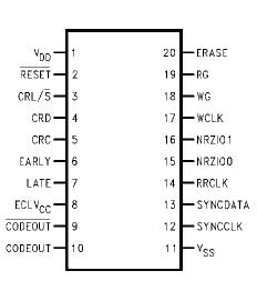 SpecificationsSupply Voltage .............. 7V
TTL Input Maximum Voltage ........7V
Maximum Output Voltage ......... 7V
ESD Susceptibility (Note 1) ...... 2000VDescriptionThe DP84902 is designed to perform the encoding and decoding for disk memory systems. DP84902 is designed to interface directly with Integrated Read Channel Products (such as National Semiconductor's DP84910) and with Disk Data Controller Products with a 2-bit NRZ interface (such as National Semiconductor's Advanced Disk Controllers). This Encoder/Decoder (ENDEC) circuit employs a 2/3 (1,7) Run Length Limited (RLL) code type and supports the hard sectored format.
The DP84902 has the option of selecting either TTL or ECL compatible code output to interface with preamplifiers commonly used in high data rate applications. This is accommplished by the setting of a bit in the control register.
The DP84902 also includes write data precompensation control circuitry which detects the need for write precompensation. This circuitry issues early and late output signals necessary for precompensation. The precompensation information is generated against a 2T pattern. The precompensation circuitry can be bypassed by the setting of a bit in the control register.
A control reigster is included to configure the DP84902and to select device operation options such as output code inversion, differential code output, bypassing of the encoder, and the use of an internal write clock.
The DP84902 is available in 20-pin SO and 20-pin SSO packages.

 DP84902 Data Sheet