Features: Makes DRAM interface and refresh tasks appear virtually transparent to the CPU making DRAMs as easy to use as static RAMs
Specifically designed to eliminate CPU wait states up to 10 MHz or beyond
Eliminates 20 discrete components for significant board real estate reduction, system power savings and the elimination of chip-to-chip AC skewing
On-board ultra precise delay line
On-board high capacitive RAS, CAS, WE and Address drivers (specified driving 88 DRAMs directly)
AC specified for directly addressing up to 8 Mbytes
Low power/high speed bipolar oxide isolated process
Downward pin and function compatible with 256k DRAM Controller/Drivers DP8409A, DP8417, DP8418,and DP8419
ApplicationIf one desires a memory interface containing the DP8429 that minimizes the number of external components required,modes 5 and 1 should be used. These two modes provide:
1) Automatic access to memory (in mode 5 only one signal,RASIN, is required in order to access memory)
2) Hidden refresh capability (refreshes are performed automatically while in mode 5 when non-local accesses are taking place, as determined by CS)
3) Refresh request capability (if no hidden refresh took place while RFCK was high, a refresh request is generated at the RFI/O pin when RFCK goes high)
4) Automatic forced refresh (If a refresh request is generated while in mode 5, as described above, external logic should switch the DP8429 into mode 1 to do an automaticforced refresh. No other external control signals need be issued. WAIT states can be inserted into the processor machine cycles if the system tries to access memory while the DP8429 is in mode 1 doing a forced refresh).Some items to be considered when integrating the DP8429 into a system design are:
1) The system designer should ensure that a DRAM access not be in progress when a refresh mode is entered. Similarly,one should not attempt to start an access while a refresh is in progress. The parameter tRFHRL specifies the minimum time from RFSH high to RASIN going low to initiate an access.
2) One should always guarantee that the DP8429 is enabled for access prior to initiating the access (see tCSRL1).
3) One should bring RASIN low even during non-local access cycles when in mode 5 in order to maximize the chance of a hidden refresh occurring.
4) At lower frequencies (under 10 Mhz), it becomes increasingly important to differentiate between READ and WRITE cycles. RASIN generation during READ cycles can take place as soon as one knows that a processor READ access cycle has started. WRITE cycles, on the other hand, cannot start until one knows that the data to be written at the DRAM inputs will be valid a setup time before CAS (column address strobe) goes true at the DRAM inputs. Therefore, in general, READ cycles can be initiated earlier than WRITE cycles.
5) Many times it is possible to only add WAIT states during READ cycles and have no WAIT states during WRITE cycles. This is because it generally takes less time to write data into memory than to read data from memory.The DP84XX2 family of inexpensive preprogrammed medium Programmable Array Logic devices (PALs) have been developed to provide an easy interface between various microprocessors and the DP84XX family of DRAM controller/drivers. These PALs interface to all the necessary control signals of the particular processor and the DP8429. The PAL controls the operation of the DP8429 in modes 5 and 1,while meeting all the critical timing considerations discussed above. The refresh clock, RFCK, may be divided down from the processor clock using an IC counter such as the DM74LS393 or the DP84300 programmable refresh timer.The DP84300 can provide RFCK periods ranging from 15.4 ms to 15.6 ms based on an input clock of 2 to 10 MHz.Figure 8 shows a general block diagram for a system using the DP8429 in modes 1 and 5. Figure 9 shows possible timing diagrams for such a system (using WAIT to prohibit access when refreshing). Although the DP84XX2 PALs are offered as standard peripheral devices for the DP84XX DRAM controller/drivers, the programming equations for these devices are provided so the user may make minor modifications for unique system requirements.
ADVANTAGES OF DP8429 OVER
A DISCRETE DYNAMIC RAM CONTROLLER
1) The DP8429 system solution takes up much less board space because everything is on one chip (latches, refresh counter, control logic, multiplexers, drivers, and internal delay lines).
2) Less effort is needed to design a memory system. The DP8429 has automatic modes (1 and 5) which require a minimum of external control logic. Also programmable array logic devices (PALs) have been designed which allow an easy interface to most popular microprocessors (Motorola 68000 family, National Semiconductor 32032 family,Intel 8086 family, and the Zilog Z8000 family).
3) Less skew in memory timing parameters because all critical components are on one chip (many discrete drivers specify a minimum on-chip skew under worst-case conditions,but this cannot be used if more then one driver is needed, such as would be the case in driving a large dynamic RAM array).
4) Our switching characteristics give the designer the critical timing specifications based on TTL output levels (low e 0.8V, high e 2.4V) at a specified load capacitance. All timing parameters are specified on the DP8429:A) driving 88 DRAM's over a temperature range of 0±70 degrees centigrade (no extra drivers are needed).
B) under worst-case driving conditions with all outputs switching simultaneously (most discrete drivers on the market specify worst-case conditions with only one output switching at a time; this is not a true worst-case condition!).
Pinout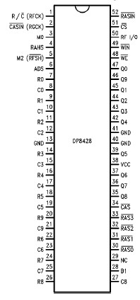 SpecificationsSupply Voltage, VCC............................................. 7.0V
Storage Temperature Range............ -65 to -150
Input Voltage ........................................................5.5V
Output Current................................................. 150 mA
Lead Temp. (Soldering, 10 seconds).................... 300DescriptionThe DP8428 and DP8429 1M DRAM Controller/Drivers are designed to provide ``No-Waitstate'' CPU interface to Dynamic RAM arrays of up to 8 Mbytes and larger. The DP8428 and DP8429 are tailored for 32-bit and 16-bit system requirements, respectively. The DP8428 and DP8429 are fabricated using National's new oxide isolated Advanced Low power Schottky (ALS) process and use design techniques which enable them to significantly out-perform all other LSI or discrete alternatives in speed, level of integration, and power consumption.
The DP8428 and DP8429 integrate the following critical 1M DRAM controller functions on a single monolithic device: ultra precise delay line; 9 bit refresh counter; fall-through row, column,and bank select input latches; Row/Column address muxing
logic; on-board high capacitive-load RAS, CAS, Write Enable and Address output drivers; and, precise control signal timing for all the above.
In order to specify the DP8428 and DP8429 for ``true'' worst case operating conditions, all timing parameters are guaranteed while the chip is driving the capacitive load of 88 DRAMs including trace capacitance. The chip's delay timing logic makes use of a patented new delay line technique which keeps AC skew to g3 ns over the full VCC range of g10% and temperature range of b55§C to a125§C. The DP8428 and DP8429 guarantee a maximum RASIN to CASOUT delay of 80 ns or 70 ns even while driving an 8 Mbyte memory array with error correction check bits included. Two speed selected options of these devices are shown in the switching characteristics section of this document.
With its four independent RAS outputs and ten multiplexed address outputs, the DP8429 can support up to four banks of 64k, 256k or 1M DRAMs. Two bank select pins, B1 and B0, are decoded to activate one of the RAS signals during an access, leaving the three non-selected banks in the standby mode (less than one tenth of the operating power) with data outputs in TRI-STATEÉ. The DP8428's one Bank Select pin, B1, enables 2 banks automatically during an access in order to provide an optimum interface for 32-bit microprocessors.The DP8428 and DP8429 each have two mode-select pins,allowing for two refresh modes and two access modes. Refresh and access timing may be controlled either externally or automatically. The automatic modes require a minimum of input control signals.
A refresh counter is on-chip and is multiplexed with the row and column inputs. Its contents appear at the address outputs of the DP8428 or DP8429 during any refresh, and are incremented at the completion of the refresh. Row, Column and bank address latches are also on-chip. However, if the address inputs to the DP8428 or DP8429 are valid throughout the duration of the access, these latches may be operated in the fall-through mode.Each device( DP8428 and DP8429) is available in either the 52 pin Ceramic DIP, or the low cost JEDEC standard 68 pin Plastic Chip Carrier (PCC) package.

 DP8428/NS32828 Data Sheet