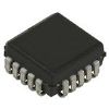
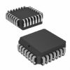
Features: • 10-MHz 200-MHz output operation• Output-to-output skews < 350 ps• 13 LVTTL 50% duty-cycle outputs capable of driving 50 terminated lines• Phase-locked loop (PLL) LOCK indicator• 3.3V LVTTL/LV differential (LVPECL) hot insertable reference inputs•...
CY7B9973V: Features: • 10-MHz 200-MHz output operation• Output-to-output skews < 350 ps• 13 LVTTL 50% duty-cycle outputs capable of driving 50 terminated lines• Phase-locked loop (P...
SeekIC Buyer Protection PLUS - newly updated for 2013!
268 Transactions
All payment methods are secure and covered by SeekIC Buyer Protection PLUS.
The CY7B9973V Low-Voltage PLL Clock Buffer offers user-selectable frequency control over system clock functions. CY7B9973V twelve output clock driver provides the system integrator selectable frequency ratios of 1:1, 2:1, 3:1, 3:2, 4:3, 5:1, 5:2, 5:3, 6:1 and 6:5 between outputs.
An additional output of CY7B9973V is dedicated to providing feedback information to allow the internal PLL to multiply an external reference frequency by 4, 6, 8, 10, 12, 16 or 20. The completely integrated PLL reduces jitter and simplifies board layout. The thirteen configurable outputs of CY7B9973V can each drive terminated transmission lines with impedances as low as 50 while delivering minimal and specified output skews at LVTTL levels.
The CY7B9973V has a flexible reference input scheme with three different hot-insertion capable inputs. These inputs allow the use of either differential LVPECL or single-ended LVTTL inputs which can be dynamically selected to provide the reference frequency.