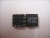
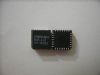
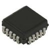
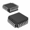
Packaging
:
Number of Circuits
: 1
Supply Voltage - Max
: 3.63 V
Supply Voltage - Min
: 2.97 V
Type
: Zero Delay PLL Clock Buffer
Maximum Operating Temperature
: + 70 C
Minimum Operating Temperature
: 0 C
Maximum Input Frequency
: 200 MHz
Minimum Input Frequency
: 24 MHz
Output Frequency Range
: 24 MHz to 200 MHz
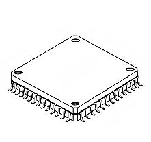
Package / Case
: TBGA-100
Features: • 500-ps max. Total Timing Budget™ (TTB™) window
• 12100-MHz (CY7B993V), or 24200-MHz (CY7B994V)
input/output operation
• Matched pair output skew < 200 ps
• Zero input-to-output delay
• 18 LVTTL outputs driving 50 terminated lines
• 16 outputs at 200 MHz: Commercial temperature
• 6 outputs at 200 MHz: Industrial temperature
• 3.3V LVTTL/LVPECL, fault-tolerant, and hot insertable
reference inputs
• Phase adjustments in 625-/1300-ps steps up to ± 10.4 ns
• Multiply/divide ratios of 16, 8, 10, 12
• Individual output bank disable
• Output high-impedance option for testing purposes
• Fully integrated phase-locked loop (PLL) with lock indicator
• Low cycle-to-cycle jitter (< 100-ps peak-peak)
• Single 3.3V ± 10% supply
• 100-pin TQFP package
• 100-lead BGA packagePinout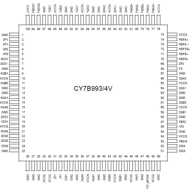 Specifications(Above which the useful life may be impaired. For user guidelines,
not tested.)
Storage Temperature ................................40°C to + 125°C
Ambient Temperature with
Power Applied............................................40°C to + 125°C
Supply Voltage to Ground Potential .............. 0.5V to + 4.6V
DC Input Voltage....................................0.3V to VCC + 0.5V
Output Current into Outputs (LOW)............................. 40 mA
Static Discharge Voltage........................................... > 1100V
(per MIL-STD-883, Method 3015)
Latch-up Current.................................................. > ± 200 mADescriptionThe CY7B993V and CY7B994V High-speed Multi-phase PLL Clock Buffers offer user-selectable control over system clock functions. This multiple-output clock driver provides the system integrator with functions of CY7B993V and CY7B994V necessary to optimize the timing of high-performance computer and communication systems.
CY7B993V and CY7B994V feature a guaranteed maximum TTB window specifying all occurrences of output clocks with respect to the input reference clock across variations in output frequency, supply voltage, operating temperature, input edge rate, and process.
Eighteen configurable outputs of CY7B993V and CY7B994V each drive terminated transmission lines with impedances as low as 50 while delivering minimal and specified output skews at LVTTL levels. The outputs are arranged in five banks. Banks 1 to 4 of four outputs allow a divide function of 1 to 12, while simultaneously allowing phase adjustments in 6251300-ps increments up to 10.4 ns. One of the output banks of CY7B993V and CY7B994V also includes an independent clock invert function. The feedback bank consists of two outputs, which allows divide-by functionality from 1 to 12 and limited phase adjustments. Any one of these eighteen outputs can be connected to the feedback input as well as driving other inputs.
Selectable reference input is a fault tolerance feature which allows smooth change over to secondary clock source, when the primary clock source is not in operation. The reference inputs and feedback inputs of CY7B993V and CY7B994V are configurable to accommodate both LVTTL or Differential (LVPECL) inputs. The completely integrated PLL reduces jitter and simplifies board layout
Parameters: | Technical/Catalog Information | CY7B994V-2BBC |
| Vendor | Cypress Semiconductor Corp |
| Category | Integrated Circuits (ICs) |
| Type | PLL Clock Buffer |
| Voltage - Supply | 3 V ~ 3.6 V |
| Number of Outputs | 18 |
| Input | LVPECL, LVTTL |
| Output | LVTTL |
| Frequency-Max | 200MHz |
| Package / Case | 100-BGA |
| Packaging | Tray |
| Operating Temperature | 0°C ~ 70°C |
| Lead Free Status | Contains Lead |
| RoHS Status | RoHS Non-Compliant |
| Other Names | CY7B994V 2BBC
CY7B994V2BBC
|
 CY7B994V-2BBC Data Sheet