CY28351

Features: • Supports 333-MHz and 400-MHz DDR SDRAM• 60- 200-MHz operating frequency• Phase-locked loop (PLL) clock distribution for double data rate synchronous DRAM applications• Distributes one clock input to ten differential outputs• External feedback pin (FBIN) i...

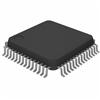
product image

CY28351 Picture
SeekIC No. : 004319233 Detail

CY28351: Features: • Supports 333-MHz and 400-MHz DDR SDRAM• 60- 200-MHz operating frequency• Phase-locked loop (PLL) clock distribution for double data rate synchronous DRAM applications&...

floor Price/Ceiling Price

Part Number:
CY28351
Supply Ability:
5000

Price Break

  • Qty
  • 1~5000
  • Unit Price
  • Negotiable
  • Processing time
  • 15 Days
Total Cost: $ 0.00

SeekIC Buyer Protection PLUS - newly updated for 2013!

  • Escrow Protection.
  • Guaranteed refunds.
  • Secure payments.
  • Learn more >>

Month Sales

268 Transactions

Rating

evaluate  (4.8 stars)

Upload time: 2024/7/15

Payment Methods

All payment methods are secure and covered by SeekIC Buyer Protection PLUS.

Notice: When you place an order, your payment is made to SeekIC and not to your seller. SeekIC only pays the seller after confirming you have received your order. We will also never share your payment details with your seller.
Product Details

Description


Features:

• Supports 333-MHz and 400-MHz DDR SDRAM
• 60- 200-MHz operating frequency
• Phase-locked loop (PLL) clock distribution for double data rate synchronous DRAM applications
• Distributes one clock input to ten differential outputs
• External feedback pin (FBIN) is used to synchronize the outputs to the clock input
• Conforms to the DDRI specification
• Spread Aware for electromagnetic interference (EMI) reduction
• 48-pin SSOP package


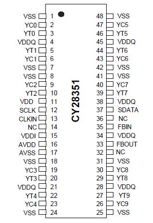
Pinout

  Connection Diagram


Specifications

Input Voltage Relative to VSS:.............................. VSS 0.3V
Input Voltage Relative to VDDQ or AVDD: ............. VDD + 0.3V
Storage Temperature: ................................65°C to +150°C
Operating Temperature: ...................................0°C to +70°C
Maximum Power Supply: .................................................3.5V


Description

This PLL clock buffer is designed for 2.5-VDD and 2.5-AVDD operation and differential outputs levels.

This CY28351 is a zero delay buffer that distributes a clock input (CLKIN) to ten differential pairs of clock outputs (YT[0:9], YC[0:9]) and one feedback clock output (FBOUT). The clock outputs are individually controlled by the serial inputs SCLK and SDATA.

The two-line serial bus can set each output clock pair (YT[0:9], YC[0:9]) to the Hi-Z state. When AVDD is grounded, the PLL is turned off and bypassed for the test purposes.

The PLL in CY28351 uses the input clock (CLKIN) and the feedback clock (FBIN) to provide high-performance, low-skew, low-jitter output differential clocks.


Customers Who Bought This Item Also Bought

Margin,quality,low-cost products with low minimum orders. Secure your online payments with SeekIC Buyer Protection.
Static Control, ESD, Clean Room Products
Optical Inspection Equipment
Inductors, Coils, Chokes
Cable Assemblies
Transformers
Boxes, Enclosures, Racks
View more