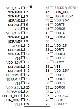
Features: • Phase-lock loop clock distribution for DDR and SDR SDRAM applications• One-single-end clock input to 6 pairs DDR outputs or 13 SDR outputs.• External feedback pins FBIN_SDR/FBOUT_SDR are used to synchronize the outputs to the clock input for SDR.• External feedb...
CY28343: Features: • Phase-lock loop clock distribution for DDR and SDR SDRAM applications• One-single-end clock input to 6 pairs DDR outputs or 13 SDR outputs.• External feedback pins FBIN...
SeekIC Buyer Protection PLUS - newly updated for 2013!
268 Transactions
All payment methods are secure and covered by SeekIC Buyer Protection PLUS.
• Phase-lock loop clock distribution for DDR and SDR SDRAM applications
• One-single-end clock input to 6 pairs DDR outputs or 13 SDR outputs.
• External feedback pins FBIN_SDR/FBOUT_SDR are used to synchronize the outputs to the clock input for SDR.
• External feedback pins FBIN_SDR/FBOUT_SDR are used to synchronize the outputs to the clock input for DDR.
• SMBus interface enables/disables outputs.
• Conforms to JEDEC SDR/DDR specifications
• Low jitter, low skew
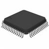
• 48 pin SSOP package
Maximum Input Voltage Relative to VSS: ............... VSS 0.5V
Maximum Input Voltage Relative to VSS: ............... VSS + 0.7V
Storage Temperature: ................................65°C to + 150°C
Operating Temperature: ....................................0°C to +70°C
Maximum ESD Protection:...............................................2000V
Maximum Power Supply: ...................................................5.5V