CXA3197R

Features: • Maximum conversion rate: During PECL operation: 125MSPS During TTL operation: 100MSPS• Resolution: 10 bits• Low power consumption: 480mW (typ.)• Data input level: TTL• Clock, reset input level: TTL and PECL compatible• 2:1 multiplexed input function&...

product image

CXA3197R Picture
SeekIC No. : 004318340 Detail

CXA3197R: Features: • Maximum conversion rate: During PECL operation: 125MSPS During TTL operation: 100MSPS• Resolution: 10 bits• Low power consumption: 480mW (typ.)• Data input level:...

floor Price/Ceiling Price

Part Number:
CXA3197R
Supply Ability:
5000

Price Break

  • Qty
  • 1~5000
  • Unit Price
  • Negotiable
  • Processing time
  • 15 Days
Total Cost: $ 0.00

SeekIC Buyer Protection PLUS - newly updated for 2013!

  • Escrow Protection.
  • Guaranteed refunds.
  • Secure payments.
  • Learn more >>

Month Sales

268 Transactions

Rating

evaluate  (4.8 stars)

Upload time: 2024/6/5

Payment Methods

All payment methods are secure and covered by SeekIC Buyer Protection PLUS.

Notice: When you place an order, your payment is made to SeekIC and not to your seller. SeekIC only pays the seller after confirming you have received your order. We will also never share your payment details with your seller.
Product Details

Description


Features:

• Maximum conversion rate:
    During PECL operation: 125MSPS
    During TTL operation: 100MSPS
• Resolution: 10 bits
• Low power consumption: 480mW (typ.)
• Data input level: TTL
• Clock, reset input level: TTL and PECL compatible
• 2:1 multiplexed input function
• 1/2 frequency-divided clock output possible by the built-in clock frequency divider circuit
• Voltage output (50½ load drive possible)
• Single power supply or ±dual power supply operation
• Reset signal polarity switching function


Application

• LCD
• DDS
• HDTV
• Communications (QPSK, QAM)
• Measuring devices


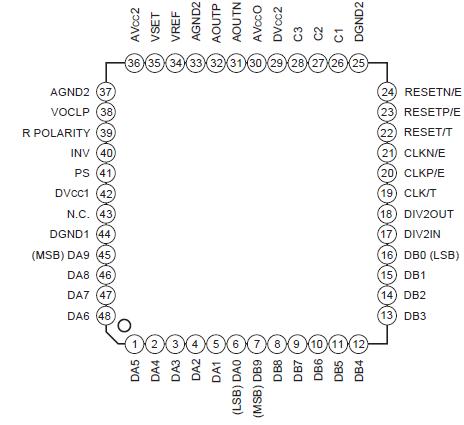
Pinout

  Connection Diagram


Specifications

• Supply voltage AVCCO, AVCC2, DVCC2..0.5 to +6.0 V
                           AGND2, DGND2 ............6.0 to +0.5 V
                           DVCC1 ..........................0.5 to +6.0 V
                           AVCC2 AGND2 ..........0.5 to +6.0 V
                           AVCCO AGND2 ..........0.5 to +6.0 V
                           DVCC2 DGND2...........0.5 to +6.0 V
• Input voltage
      (Analog)      VSET .....AGND2 0.5 to AVCC2 + 0.5 V
      (Digital)       TTL input pin ...DGND1... 0.5 to DVCC1 + 0.5 V
                         PECL input pin DGND1... 0.5 to DVCC1 + 0.5 V
                         PS DGND1 .................... 0.5 to DVCC1 + 0.5 V
     (Others)      VOCLP DGND1 .............. 0.5 to DVCC1 + 0.5 V
• Storage temperature Tstg .......................... 65 to +150 °C
• Allowable power dissipation Pd .....................................1.4 W
(when mounted on a two-layer glass fabric base epoxy board with dimensions of 76mm  *114mm, t = 1.6mm)


Description

The CXA3197R is a high-speed D/A converter which can perform multiplexed input of two system 10-bit data.

This IC realizes a maximum conversion rate of CXA3197R. Multiplexed operation is possible by inputing the 1/2 frequency-divided clock or by halving the frequency of the clock internally with the clock frequency divider circuit having the reset pin. The data input is at TTL level, and the clock input and reset input can select either TTL or PECL level according to the application.


Customers Who Bought This Item Also Bought

Margin,quality,low-cost products with low minimum orders. Secure your online payments with SeekIC Buyer Protection.
Cables, Wires
Soldering, Desoldering, Rework Products
Programmers, Development Systems
Sensors, Transducers
Motors, Solenoids, Driver Boards/Modules
View more