Features: • Single supply voltage 2.7 to 3.3 V• Operational temperature 30 °C to +85 °C• Low power consumption in all operating modes including sleep operation• Single mode for CDMA phones, but also with GPS position location capability• Receive signal path includes:&...
CX20536: Features: • Single supply voltage 2.7 to 3.3 V• Operational temperature 30 °C to +85 °C• Low power consumption in all operating modes including sleep operation• Single mode f...
SeekIC Buyer Protection PLUS - newly updated for 2013!
268 Transactions
All payment methods are secure and covered by SeekIC Buyer Protection PLUS.
The CX20536 is a receive-only Code Division Multiple Access (CDMA) and Global Positioning System (GPS) Baseband Analog Processor (BAP) for dual-mode CDMA and GPS-capable portable phones. The device is designed to interface between the receive section and the digital processing circuitry of the telephone.
The CX20536 includes all of the circuitry needed to support receive baseband signal processing and conversions between analog and digital signals for CDMA and GPS operation. For a given operation, the CX20536 accepts analog In-phase (I) and Quadrature (Q) signals, performs channel selection low-pass filtering, and converts the analog baseband signals into digital signals. For clock generation, the CX20536 includes internal digital and Phase Locked Loop (PLL) clock synthesis for 19.2, 19.68, and 19.8 MHz system clocks. It also provides the capability to accept the CHIPx8 clock from the Mobile Station Modem (MSM) or equivalent baseband device. The CX20536 also integrates a VHF PLL synthesizer to synthesize a receive Intermediate Frequency (IF) Local Oscillator (LO).
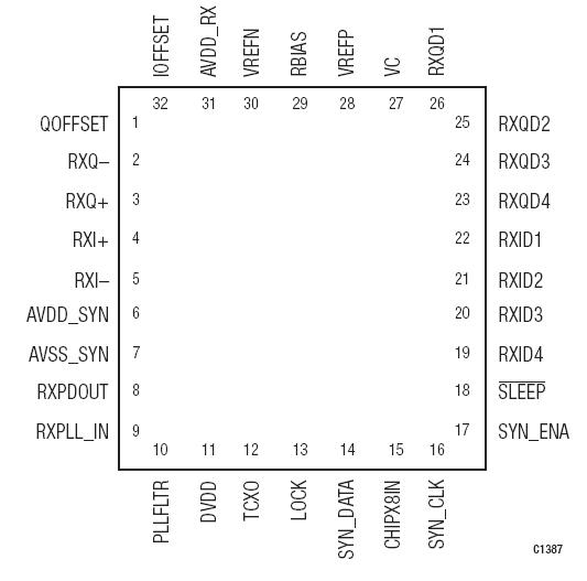
The CX20536 operates within a power supply voltage range of 2.7 V to 3.3 V. Power control logic maintains a minimum power consumption. Electrical performance parameters are designed to operate over the 30 °C to +85 °C range. The device is available in a 32-pin, 5 x 5 x 1 mm RF Land Grid Array (RFLGA) package. The device package and pinout are shown in Figure 1. A system block diagram of the CX20536 is shown in Figure 2.