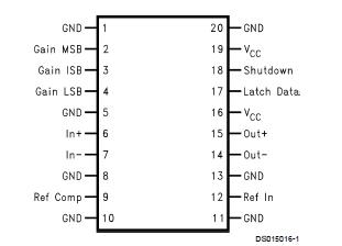
Features: ·350 MHz bandwidth·Differential input and output·Gain control: parallel w/data latching·Supply voltage: +5V·Supply current: 48 mAApplication·Cellular/PCS base stations·IF sampling receivers·Infrared/CCD imaging·Back-channel modems·Electro-optics·Instrumentation· Medical imaging·High defi...
CLC5526: Features: ·350 MHz bandwidth·Differential input and output·Gain control: parallel w/data latching·Supply voltage: +5V·Supply current: 48 mAApplication·Cellular/PCS base stations·IF sampling receiver...
SeekIC Buyer Protection PLUS - newly updated for 2013!
268 Transactions
All payment methods are secure and covered by SeekIC Buyer Protection PLUS.
The CLC5526 is a high performance, digitally controlled, variable-gain amplifier (DVGA). It has been designed for use in a broad range of mixed signal and digital communication applications such as mobile radio, cellular base stations and back-channel modems where automatic-gain-control (AGC) is required to increase system dynamic range.
The CLC5526 has differential input and output, allowing large signal swings on a single 5V rail. The input impedance is 200W. The differential output impedance is 600W and is designed to drive a 1 k differential load. The output amplifier has excellent intermodulation performance. The CLC5526 is designed to accept signals from RF elements and maintain a terminated impedance environment.
The CLC5526 maintains a 350 MHz bandwidth over its entire gain and attenuation range from +30 dB to −12 dB. Internal clamping ensures very fast overdrive recovery. Two tone intermodulation distortion is excellent: at 150 MHz, 1 Vpp it is −64 dBc.
Input signals to the CLC5526 are scaled by an accurate, differential R-2R resistive ladder with an input impedance of 200W. A scaled version of the input is selected under digital control and passed to the internal amplifier. The input common mode level is set at 2.4V via a bandgap referenced bias generator which can be overridden by an external input.
Following the resistive ladder is a fixed, 30 dB gain amplifier. The output stage common mode voltage of the CLC5526 is set to 3V, by internal, positive supply connected resistors. Digital control of the CLC5526 is accomplished by a 3-bit parallel gain control input and a data valid pin to latch the data. If the data is not latched, the DVGA is transparent to gain control updates. All digital inputs are TTL/CMOS compatible.