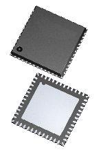
Pinout Description
The CDCLVP215 clock driver distributes two times one differential clock pair of LVPECL, (CLKA, CLKB) to 5 pairs of differential LVPECL clock (QA0..QA4, QB0..QB4) outputs with minimum skew for clock distribution. The CDCLVP215 specifies low output-to-output skew. The CDCLVP215 is specifically designed for driving 50-Ω transmission lines. When an output pair is not used, leaving it open is recommended to reduce power consumption. If only one of the output pairs is used, the other output pair must be identically terminated to 50 Ω.
Features of the CDCLVP215 are:(1)2* One Differential Clock Input Pair LVPECL to 5 Differential LVPECL Clock Outputs; (2)Fully Compatible With LVPECL/LVECL; (3)Supports a Wide Supply Voltage Range From 2.375 V to 3.8 V; (4)Open Input Default State; (5)Low-Output Skew (Typ 15 ps) for Clock-Distribution Applications; (6)VBB Reference Voltage Output for Single-Ended Clocking; (7)Available in the QFN32 Package; (8)Frequency Range From DC to 3.5 GHz; (9)Pin-to-Pin Compatible With the MC100 Series EP111, LVEP210, ES6111, LVEP111.
The absolute maximum ratings of the CDCLVP215 can be summarized as:(1)Supply voltage (relative to VEE): 0.3 to 4.6 V; (2)Input voltage: 0.3 to VCC + 0.5 V; (3)Output voltage: 0.3 to VCC + 0.5 V; (4)Input current :±20 mA; (5)Negative supply voltage (relative to VCC): -4.6 to 0.3 V; (6)Sink/source current: 1 to 1 mA; (7)DC output current: 50 mA; (8)Storage temperature range: 65 to 150 °C.
If you want to know more CDCLVP215 information such as the electrical characteristics ,please download the datasheet in www.seekdatasheet.com .

 CDCLVP215 Data Sheet


