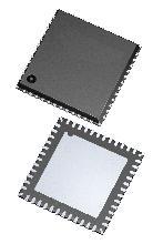
Pinout Description
The CDCL1810 is a high-performance clock distributor. The programmable dividers, P0 and P1 give a high flexibility to the ratio of the outpu frequency to the input frequency:F OUT = F IN /P Where:P (P0,P1) = 1, 2, 4, 5, 8, 10, 16, 20, 32, 40, 80 .The CDCL1810 supports one differential LVDS clock input and a total of 10 differential CML outputs. The CML outputs are compatible with LVDS receivers if they are ac-coupled.
Features of the CDCL1810 are:(1)Single 1.8V Supply; (2)High-Performance Clock Distributor with 10 Outputs; (3)Low Input-to-Output Additive Jitter:As Low As 10fs RMS; (4)Output Group Phase Adjustment; (5)Low-Voltage Differential Signaling (LVDS) Input, 100 Differential On-Chip Termination, Up to 650MHz Frequency; (6)Differential Current Mode Logic (CML) Outputs, 50 ? Single-Ended On-Chip Termination, Up to 650MHz Frequency; (7)Two Groups of Five Outputs Each with Independent Frequency Division Ratios; (8)Output Frequency Derived with Divide Ratios of 1, 2, 4, 5, 8, 10, 16, 20, 32, 40, and 80; (9)Meets ANSI TIA/EIA-644-A-2001 LVDS Standard Requirements.
The absolute maximum ratings of the CDCL1810 can be summarized as:(1)Supply voltage (2): 0.3 to 2.5 V; (2)Voltage range at LVDS input pins (2): 0.3 to 4.0 V; (3)Voltage range at all non-LVDS input pins (2): 0.3 to 3.0 V; (4)Electrostatic discharge (HBM) :2 kV; (5)Junction temperature :+125 ° C; (6)Storage temperature range: 65 to +150 ° C.
If you want to know more CDCL1810 information such as the electrical characteristics ,please download the datasheet in www.seekdatasheet.com .

 CDCL1810 Data Sheet


