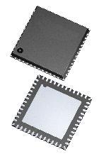
Pinout Description
The CDCLVP2108 is a highly versatile, low additive jitter buffer that can generate 16 copies of LVPECL clock outputs from two LVPECL, LVDS, or LVCMOS inputs for a variety of communication applications. It has a maximum clock frequency up to 2 GHz. Each buffer block consists of one input that feeds two LVPECL outputs. The overall additive jitter performance is less than 0.1 ps, RMS from 10 kHz to 20 MHz, and overall output skew is as low as 25 ps, making the device a perfect choice for use in demanding applications.
Features of the CDCLVP2108 are:(1)Dual 1:8 Differential Buffer; (2)Two Clock Inputs; (3)Universal Inputs Can Accept LVPECL, LVDS,LVCMOS/LVTTL; (4)16 LVPECL Outputs; (5)Maximum Clock Frequency: 2 GHz; (6)Maximum Core Current Consumption: 115 mA; (7)Very Low Additive Jitter: < 100 fs,rms in 10-kHz to 20-MHz Offset Range; (8)2.375 V to 3.6 V Device Power Supply; (9)Maximum Propagation Delay: 550 ps; (10)Maximum Within Bank Output Skew: 25 ps; (11)LVPECL Reference Voltage, V AC_REF , Available for Capacitive-Coupled Inputs.
The absolute maximum ratings of the CDCLVP2108 can be summarized as:(1)Supply voltage range (2): 0.5 to 4.6 V; (2)Input voltage range (3): 0.5 to V CC + 0.5 V; (3)Output voltage range (3): 0.5 to V CC + 0.5 V; (4)Input current :20 mA; (5)Output current :50 mA; (6)Specified free-air temperature range (no airflow): 40 to +85 ° C; (7)Storage temperature range: 65 to +150 ° C; (8)Maximum junction temperature: +125 ° C; (9)Electrostatic discharge (HBM): 2 kV.
If you want to know more CDCLVP2108 information such as the electrical characteristics ,please download the datasheet in www.seekdatasheet.com .

 CDCLVP2108 Data Sheet


