CDCLVD1212

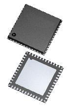
PinoutDescriptionThe CDCLVD1212 clock buffer distributes one of two selectable clock inputs (IN0, IN1) to 12 pairs of differential LVDS clock outputs (OUT0, OUT11) with minimum skew for clock distribution. The CDCLVD1212 can accept two clock sources into an input multiplexer. The inputs can either...

product image

CDCLVD1212 Picture
SeekIC No. : 004312286 Detail

CDCLVD1212: PinoutDescriptionThe CDCLVD1212 clock buffer distributes one of two selectable clock inputs (IN0, IN1) to 12 pairs of differential LVDS clock outputs (OUT0, OUT11) with minimum skew for clock distri...

floor Price/Ceiling Price

Part Number:
CDCLVD1212
Supply Ability:
5000

Price Break

  • Qty
  • 1~5000
  • Unit Price
  • Negotiable
  • Processing time
  • 15 Days
Total Cost: $ 0.00

SeekIC Buyer Protection PLUS - newly updated for 2013!

  • Escrow Protection.
  • Guaranteed refunds.
  • Secure payments.
  • Learn more >>

Month Sales

268 Transactions

Rating

evaluate  (4.8 stars)

Upload time: 2024/10/17

Payment Methods

All payment methods are secure and covered by SeekIC Buyer Protection PLUS.

Notice: When you place an order, your payment is made to SeekIC and not to your seller. SeekIC only pays the seller after confirming you have received your order. We will also never share your payment details with your seller.
Product Details

Description


Pinout

  Connection Diagram


Description

The CDCLVD1212 clock buffer distributes one of two selectable clock inputs (IN0, IN1) to 12 pairs of differential LVDS clock outputs (OUT0, OUT11) with minimum skew for clock distribution. The CDCLVD1212 can accept two clock sources into an input multiplexer. The inputs can either be LVDS, LVPECL, or LVCMOS.

Features of the CDCLVD1212 are:(1)2:12 Differential Buffer; (2)Low Additive Jitter: <300 fs RMS in 10 kHz to 20 MHz; (3)Low Output Skew of 50 ps (Max); (4)Universal Inputs Accept LVDS, LVPECL,LVCMOS; (5)Selectable Clock Inputs Through Control Pin; (6)12 LVDS Outputs, ANSI EIA/TIA-644A Standard Compatible; (7)Clock Frequency up to 800 MHz; (8)2.3752.625 V Device Power Supply; (9)LVDS Reference Voltage, VAC_REF, Available for Capacitive Coupled Inputs; (10)Industrial Temperature Range 40°C to 85°C; (11)Packaged in 6mm * 6mm 40-Pin QFN (RHA); (12)ESD Protection Exceeds 3 kV HBM, 1 kV CDM.

The absolute maximum ratings of the CDCLVD1212 can be summarized as:(1)Supply voltage range, VCC: 0.3 to 2.8 V; (2)Input voltage range, VI: 0.2 to (VCC + 0.2) V; (3)Output voltage range, VO :0.2 to (VCC + 0.2) V; (4)Driver short circuit current, IOSD :See Note (2); (5)Electrostatic discharge (Human Body Model, 1.5 k, 100 pF):>3000 V.

If you want to know more CDCLVD1212 information such as the electrical characteristics ,please download the datasheet in www.seekdatasheet.com .


Customers Who Bought This Item Also Bought

Margin,quality,low-cost products with low minimum orders. Secure your online payments with SeekIC Buyer Protection.
Industrial Controls, Meters
Soldering, Desoldering, Rework Products
Programmers, Development Systems
LED Products
Discrete Semiconductor Products
View more