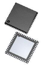
CDCLVC1112

PinoutDescriptionThe CDCLVC1112 is a modular, high-performance, low-skew, general purpose clock buffer family from Texas Instruments.The whole family is designed with a modular approach in mind. It is intended to round up TI's series of LVCMOS clock generators.There are 7 different fan-out variati...

product image

CDCLVC1112 Picture
SeekIC No. : 004312283 Detail

CDCLVC1112: PinoutDescriptionThe CDCLVC1112 is a modular, high-performance, low-skew, general purpose clock buffer family from Texas Instruments.The whole family is designed with a modular approach in mind. It ...

floor Price/Ceiling Price

Part Number:
CDCLVC1112
Supply Ability:
5000

Price Break

  • Qty
  • 1~5000
  • Unit Price
  • Negotiable
  • Processing time
  • 15 Days
Total Cost: $ 0.00

SeekIC Buyer Protection PLUS - newly updated for 2013!

  • Escrow Protection.
  • Guaranteed refunds.
  • Secure payments.
  • Learn more >>

Month Sales

268 Transactions

Rating

evaluate  (4.8 stars)

Upload time: 2024/11/21

Payment Methods

All payment methods are secure and covered by SeekIC Buyer Protection PLUS.

Notice: When you place an order, your payment is made to SeekIC and not to your seller. SeekIC only pays the seller after confirming you have received your order. We will also never share your payment details with your seller.
Product Details

Description


Pinout

  Connection Diagram


Description

The CDCLVC1112 is a modular, high-performance, low-skew, general purpose clock buffer family from Texas Instruments.The whole family is designed with a modular approach in mind. It is intended to round up TI's series of LVCMOS clock generators.There are 7 different fan-out variations, 1:2 to 1:12, available. All of the devices are pin compatible to each other for easy handling.All family members share the same high performing characteristics like low additive jitter, low skew, and wide operating temperature range.

Features of the CDCLVC1112 are:(1)High-Performance 1:2, 1:3, 1:4, 1:6, 1:8, 1:10,1:12 LVCMOS Clock Buffer Family; (2)Very Low Pin-to-Pin Skew < 50 ps; (3)Very Low Additive Jitter < 100 fs; (4)Supply Voltage: 3.3 V or 2.5 V; (5)fmax = 250 MHz for 3.3 V fmax = 180 MHz for 2.5 V; (6)Operating Temperature Range: 40°C to 85°C; (7)Available in 8-, 14-, 16-, 20-, 24-Pin TSSOP Package (all pin compatible).

The absolute maximum ratings of the CDCLVC1112 can be summarized as:(1)Supply voltage range 0.5 V to 4.6 V; (2)Input voltage range (2); (3)0.5 V to VDD + 0.5 V; (4)Output voltage range (2); (5)0.5 V to VDD + 0.5 V; (6)Input current ±20 mA; (7)Continuous output current ±50 mA; (8)Maximum junction temperature 125°C; (9)Storage temperature range 65°C to 150°C.

If you want to know more CDCLVC1112 information such as the electrical characteristics ,please download the datasheet in www.seekdatasheet.com .


Customers Who Bought This Item Also Bought

Margin,quality,low-cost products with low minimum orders. Secure your online payments with SeekIC Buyer Protection.
Isolators
Soldering, Desoldering, Rework Products
Optical Inspection Equipment
Semiconductor Modules
Fans, Thermal Management
View more