Features: Fast Read Access Time: 70/90/120/150 ns
On-Chip Address and Data Latches
Blocked Architecture:
• One 8 KB Boot Block w/ Lock Out
--Top or Bottom Locations
•Two 4 KB Parameter Blocks
•One 112 KB Main Block
Low Power CMOS Operation
12.0V ± 5% Programming and Erase Voltage
Automated Program & Erase Algorithms
High Speed Programming
Commercial, Industrial and Automotive Temperature Ranges
Deep Powerdown Mode
•0.05 mA ICC Typical
• 0.8 mA IPP Typical
Hardware Data Protection
Electronic Signature
100,000 Program/Erase Cycles and 10 Year Data Retention
JEDEC Standard Pinouts:
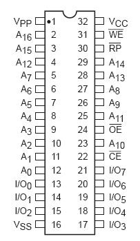
•32 pin DIP
• 32 pin PLCC
• 32 pin TSOP
Reset/Deep Power Down Mode
Pinout Specifications
Temperature Under Bias ......................................................................................................... 55°C to +95°C
Storage Temperature ........................................................................................................... 65°C to +150°C
Voltage on Any Pin with Respect to Ground(1) ................................................................. 2.0V to +VCC + 2.0V
(Except A9, RP, OE, VCC and VPP) Voltage on Pin A9, RP AND OE with Respect to Ground(1) .... 2.0V to +13.5V
VPP with Respect to Ground during Program/Erase(1) .............................................................. 2.0V to +14.0V
VCC with Respect to Ground(1) ................................................................................................... 2.0V to +7.0V
Package Power Dissipation Capability (TA = 25°C) ................................................................................... 1.0 W
Lead Soldering Temperature (10 secs) .................................................................................................... 300°C
Output Short Circuit Current(2) ............................................................................................................... 100 mA
Description
The CAT28F001 is a high speed 128K X 8 bit electrically erasable and reprogrammable Flash memory ideally suited for applications requiring in-system or after sale code updates.
The CAT28F001 has a blocked architecture with one 8 KB Boot Block, two 4 KB Parameter Blocks and one 112 KB Main Block. The Boot Block section can be at the top or bottom of the memory map and includes a reprogramming write lock out feature to guarantee data integrity. It is designed to contain secure code which will bring up the system minimally and download code to other locations of CAT28F001.
The CAT28F001 is designed with a signature mode which allows the user to identify the IC manufacturer and device type. The CAT28F001 is also designed with on-Chip Address Latches, Data Latches, Programming and Erase Algorithms.
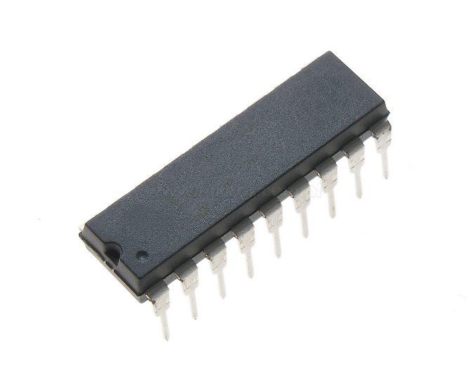
The CAT28F001 is manufactured using Catalyst's advanced CMOS floating gate technology. It is designed to endure 100,000 program/erase cycles and has a data retention of 10 years. The device is available in JEDEC approved 32-pin plastic DIP, PLCC or TSOP packages.

 CAT28F001 Data Sheet


