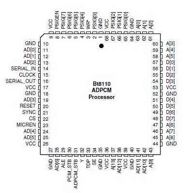
Features: • Bt8110B offers internal ROM
• 24 or 32 full-duplex channel capacity (48 or 64 channels with two processors)
• 2-, 3-, 4- and 5-bit quantization dynamically selectable on a channel-by-channel, frame-by-frame basis
• Transparent channel operation
• Two control modes available: microprocessor and hardware.
• Direct framer interface for both T1 and E1 signal formats
• Supports the optimal RESET function described in the algorithm standards
• Supports even-bit inversion of A-law inputs and outputs (required by ITU-T Recommendations G.726, and G.727)
• Minimum throughput delay
• Pin compatible with Bt8110
• 8 mw per-channel, low-power CMOSApplication• T1/E1 Transcoders
• T1/E1 Multiplexers
• Personal Communications Systems:
Digital European Cordless
Telecommunications (DECT),
Personal Access Communications
System (PACS)
• Wireless Local Loop
• Voice PairGain
• DCME Systems
• Speech Processing/Recording
• Voice Mail/Packetization
• Voice over ATM/Frame RelayPinout Specifications
The power consumption is proportional to the internal Bt8110/8110B system clock rate as shown in Table 4-5; however, the ROM power is not included.
Stresses above those listed as Absolute Maximum Ratings may cause permanent damage to the device. This is a stress rating only, and functional operation of the device at these or any other conditions above those indicated in the other sections of this document is not implied. Exposure to absolute maximum rating conditions for extended periods may affect device reliability.
This device should be handled as an ESD-sensitive device. Voltage on any signal pin that exceeds the power supply voltage by more than +0.5 V can induce destructive latchup.
| Parameter |
Symbol |
Value |
Unit |
| Supply Voltage |
VDD |
0.5 to +7.0 |
Volts |
| Input Voltage |
VIN |
0.5 to VDD +0.5 |
Volts |
| Output Voltage |
VOUT |
0.5 to VDD +0.5 |
Volts |
| Operating Temperature |
TA |
40 to +85 |
|
| Storage Temperature |
TSTG |
55 to +150 |
|
| Operating Supply Voltage |
VCC |
+4.75 to +5.25 |
Volts |
Bt8110:
Maximum Current @ 8.192 MHz (internal clk) |
ICC |
96 |
mA |
Bt8110B:
Maximum Current @ 8.192 MHz (internal clk) |
ICC |
50 |
mA |
DescriptionThe Adaptive Differential Pulse Code Modulation (ADPCM) algorithm Bt8110B is a transcoding operation which consists of encoding 64 kbit/s Pulse Code Modulation (PCM) to 16, 24, 32, or 40 kbit/s ADPCM and decoding from ADPCM to 64 kbit/s PCM. The multichannel processor provides transcoding for both A-law and -law PCM codes. The PCM coding rate is selectable on a channel-by-channel basis.
The Bt8110/8110B has a maximum capacity of 64 channels of ADPCM operations. Bt8110B can be configured to provide 24 or 32 full-duplex channels providing both encoding and decoding. It can also be configured to provide 48 or 64 half-duplex channels providing either encoding or decoding. The Bt8110/8110B consists of a VLSI CMOS integrated circuit and a ROM.
NOTE: In the Bt8110, the ROM is external. Additionally, for the Bt8110, a 64 K ROM will provide six different ADPCM codes, while a 128 K ROM will provide 14 different ADPCM codes. (See Table 3-1.). The Bt8110B has an internal ROM or can be used with the external ROM. The Bt8110B's internal ROM contains 14 different ADPCM codes (see Table 3-2),
Two Bt8110/8110Bs and a single ROM can be configured to provide 48 or 64 full-duplex channels for operation in transcoding applications. There are two control modes for the Bt8110/8110B: Hardware and Microprocessor. The hardware mode provides for input of code selection, transparency selection, algorithm reset, and PCM coding law on a per-channel basis. The microprocessor mode is provided via an integral interface to a microprocessor consisting of a microprocessor, program and data memory, and desired status indicators.

 Bt8110B Data Sheet


