Crosstalk
:
Bandwidth
:
On Time (Max)
:
Off Time (Max)
:
Switch Voltage (Max)
:
Operating Supply Voltage
:
Number of Switches
:
Switch Configuration
:
Mounting Style
: SMD/SMT
Maximum Operating Temperature
: + 150 C
On Resistance (Max)
: 0.014 Ohms
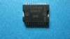
Package / Case
: DSO-20
Application• µC compatible high-side power switch with diagnostic feedback for 12V and 24V grounded loads
• All types of resistive, inductive and capacitve loads
• Most suitable for loads with high inrush currents, so as lamps
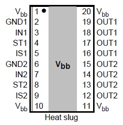
• Replaces electromechanical relays, fuses and discrete circuitsPinout
 Specifications
| Parameter |
Symbol |
Values |
Unit |
| Supply voltage (overvoltage protection see page 5) |
Vbb |
43 |
V |
Supply voltage for full short circuit protection
Tj,start =-40 ...+150°C |
Vbb |
34 |
V |
| Load current (Short-circuit current, see page 5) |
IL |
self-limited |
A |
Load dump protection1) VLoadDump = UA + Vs, UA = 13.5 V
RI2)= 2,td= 200 ms, IN= low or high
each channel loaded with RL = 1.0, |
VLoaddump3) |
60 |
V |
Operating temperature range
Storage temperature range |
Tj
Tstg |
-40 ...+150
-55 ...+150 |
°C |
Power dissipation (DC)4) Ta = 25°C:
(all channels active) Ta = 85°C: |
Ptot |
3.8
2.0 |
W |
Maximal switchable inductance, single pulse
Vbb =12V, Tj,start =150°C4),
IL = 4 A, EAS = 1.13J, 0 one channel:
IL = 12A, EAS = 430 mJ, 0 one channel:
IL = 24A, EAS = 800 mJ, 0 two parallel channels:
see diagrams on page 10 |
ZL |
100
4.4
2.0 |
mH |
Electrostatic discharge capability (ESD) IN:
(Human Body Model) ST,IS:
out to all other pins shorted:
acc. MIL-STD883D, method 3015.7 and ESD assn. std. S5.1-1993
R=1.5k; C=100pF |
VESD |
1.0
4.0
8.0 |
kV |
| Input voltage (DC) |
VIN |
-10 ... +16 |
V |
Current through input pin (DC)
Current through status pin (DC)
Current through current sense pin (DC)
see internal circuit diagram page 9 |
IIN
IST
IIS |
±2.0
±5.0
±14 |
mA |
DescriptionThe BTS840S2 is designed as one kind of smart high-side power switch.N channel vertical power MOSFET with charge pump,ground referenced CMOS compatible input,diagnostic feedback and proportional load current sense monolithically integrated in Smart SIPMOS technology.Also it providing embedded protective functions.
The BTS840S2 can be used in (1)µC compatible high-side power switch with diagnostic feedback for 12V and 24V grounded loads;(2)all types of resistive, inductive and capacitve loads;(3)most suitable for loads with high inrush currents,so as lamps;(4)replaces electromechanical relays, fuses and discrete circuits.
Basic functions of the BTS840S2 are:(1)logic ground independent from load ground;(2)fast demagnetization of inductive loads;(3)undervoltage and over voltage shutdown with auto-restart and hysteresis;(4)CMOS compatible input.And the absolute maximum ratings of the BTS840S2 can be summarized as:(1)supply voltage:43 V;(2)supply voltage for full short circuit protection:34 V;(3)load current:self-limited A;(4)operating temperature range:-40 to +150°C;(5)storage temperature range:-55 to +150°C;(6)input voltage (DC):-10 to +16 V;(7)current through input pin (DC):±2.0 mA;(8)current through status pin (DC):±5.0 mA.If you want to know more information about the BTS840S2,please download the datasheet in www.seekdatasheet.com .
The BTS840S2 features are as follows:
• N channel vertical power MOSFET with charge pump, ground referenced CMOS compatible input, diagnostic feedback and proportional load current sense monolithically integrated in Smart SIPMOS
® technology.
• Providing embedded protective functions
Parameters: | Technical/Catalog Information | BTS840S2 |
| Vendor | Infineon Technologies (VA) |
| Category | Integrated Circuits (ICs) |
| Package / Case | DSO-20 |
| Mounting Type | Surface Mount |
| Type | High Side |
| Voltage - Supply | 5 V ~ 34 V |
| On-State Resistance | 27 mOhm |
| Current - Output / Channel | 12A |
| Current - Peak Output | 50A |
| Packaging | Digi-Reel? |
| Input Type | Non-Inverting |
| Number of Outputs | 2 |
| Operating Temperature | -40°C ~ 150°C |
| Lead Free Status | Contains Lead |
| RoHS Status | RoHS Non-Compliant |
| Other Names | BTS840S2
BTS840S2
BTS840S2INDKR ND
BTS840S2INDKRND
BTS840S2INDKR
|

 BTS840S2 Data Sheet