Features: Zero input - output propagation delay, adjustable by capacitive load on FBK input.
Multiple configurations - Refer "ASM5P2304A onfigurations Table".
Input frequency range: 15MHz to 133MHz
Multiple low-skew outputs.
Output-output skew less than 200pS.
Device-device skew less than 500pS.
Two banks of four outputs.
Less than 200pS Cycle-to-Cycle jitter (-1, -1H, -2, -2H).
Available in space saving, 8 pin 150-mil SOIC packages.
3.3V operation.
Advanced 0.35< CMOS technology.
Industrial temperature available. Pinout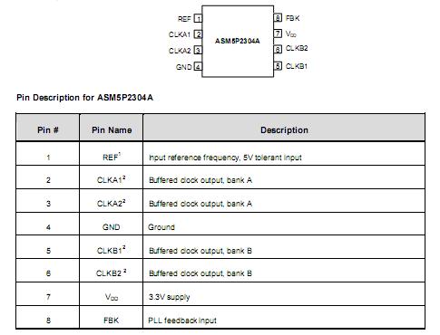 Specifications
|
Parameter |
Min |
Max |
Unit |
| Supply Voltage to Ground Potential |
-0.5 |
+7.0 |
V |
| DC Input Voltage (Except REF) |
-0.5 |
VDD + 0.5
|
V |
| DC Input Voltage (REF) |
-0.5 |
7 |
V |
| Storage Temperature |
-65 |
+150 |
V |
| Max. Soldering Temperature (10 sec) |
|
260 |
|
| Junction Temperature |
|
150 |
|
Static Discharge Voltage
(As per JEDEC STD22- A114-B) |
|
>2000 |
V |
| Note: These are stress ratings only and functional usage is not implied. Exposure to absolute maximum ratings for prolonged periods can affect device reliability. |
DescriptionASM5P2304A is a versatile, 3.3V zero-delay buffer designed to distribute high-speed clocks in PC, workstation, datacom, telecom and other high-performance applications. It is available in 8 pin package. The part has an on-chip PLL which locks to an input clock presented on the REF pin. The PLL feedback is required to be driven to FBK pin, and can be obtained from one of the outputs. The input-to-output propagation delay is guaranteed to be less than 250pS, and the output-to-output skew is guaranteed to e less than 200pS.
That has two banks of two outputs each. Multiple ASM5P2304A devices can accept the same input clock and distribute it. In this case the skew between the outputs of the two devices is guaranteed to be less than 500pS.
The ASM5P2304A is available in two different configurations (Refer !°ASM5P2304A Configurations Table).It is the base part, where the output frequencies equal the reference if there is no counter in the feedback path. The ASM5P2304A-1H is the high-drive version of the -1 and the rise and fall times on this device are much faster.
The ASM5P2304A-2 allows the user to obtain REF and 1/2X or 2X frequencies on each output bank. The exact configuration and output frequencies depend on which output drives the feedback pin.

 ASM5P2304A Data Sheet