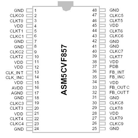
Features: • Low skew; low jitter PLL clock driver.
• 1 to 10 differential clock distribution (SSTL_2).
• Feedback pins for input to output synchronization.
• PDB for power management.
• Spread spectrum tolerant inputs.
• Auto-PD when input signal removed.
• Choice of static phase offset for easy board tuning:
• -XXX = device pattern number for options listed below:
• PCV857-025 - 0 ps
• PCV857-1300 - +50 psApplication• DDR Memory Modules / Zero Delay Board Fan Out.
• Provides complete DDR DIMM logic solution with
ASM4SSTVF16857, ASM4SSTVF16859 &
ASM4SSTVF32852.Pinout Specifications
| Parameter |
Min |
Max |
Unit |
| Supply voltage (VDD and AVDD) |
-0.5 |
3.6 |
V |
| Logic Inputs |
GND - 0.5 |
VDD + 0.5 |
V |
| Ambient Operating Temperature |
0 |
85 |
°C |
| Storage Temperature |
-65 |
150 |
°C |
| These are stress ratings only and functional operation is not implied. Exposure to absolute maximum ratings for prolonged periods may affect device reliability. |
DescriptionThis PLL clock buffer is designed for a VDD of 2.5V, AVDD of 2.5V and differential data input and output levels. ASM5CVF857 is a zero-delay buffer that distributes a differential clock input pair (CLK_INT, CLK_INC) to ten differential pairs of clock outputs (CLKT[0:9], CLKC[0:9]) and one differential pair feedback clock output (FB_OUT, FB_OUTC). The clock outputs of ASM5CVF857 are controlled by the input clocks (CLK_INT, CLKINC), the feedback clocks (FB_INT, FB_INC), the 2,5V LVCMOS input (PDB), and the analog power input (AVDD).
When input (PDB) is low while power is applied, the receivers are disabled, the PLL is turned off, and the differential clock outputs are tri-stated. When AVDD is grounded, the PLL is turned off and bypassed for test purposes. When the input frequency is less than the operating frequency of the PLL, approximately 20MHz, the device will enter a low power mode. An input frequency detection circuit on the differential inputs, independent from the input buffers, will detect the low frequency condition and perform the same low power features as and when the PDB input is low.
When the input frequency increases to greater than approximately 20MHz, the PLL ASM5CVF857 will be turned back on, the inputs and outputs will be enabled, and the PLL will obtain phase lock between the feedback clock pair (FB_INT, FB_INC) and the input clock pair (CLK_INT, CLK_INC). The PLL ASM5CVF857 in the ASM5CVF857 clock driver uses the input clocks (CLK_INT, CLKINC) and the feedback clocks (FB_INT, FB_INC) to provide high-performance, low-skew, low-jitter output differential clocks (CLKT[0:9], CLKC[0:9]). ASM5CVF857 is also able to track spread spectrum clock (SSC) for reduced EMI. ASM5CVF857 is characterized for operation from 0°C to 85°C.

 ASM5CVF857 Data Sheet


