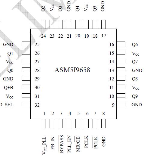
Features: 1:10 PLL based low-voltage clock generator
Supports zero-delay operation
3.3V power supply
Generates clock signals up to 250MHz
Maximum output skew of 120pS
Differential LVPECL reference clock input
External PLL feedback
Drives up to 20 clock lines
32 lead LQFP packaging
Pin and function compatible to the MPC958 and MPC9658Pinout Specifications
| Symbol |
Characteristics |
Min |
Max |
Unit |
Condition |
| VCC |
Supply Voltage |
-0.3 |
3.9 |
V |
|
| VIN |
DC Input Voltage |
-0.3 |
VCC+0.3 |
V |
|
| VOUT |
DC Output Voltage |
-0.3 |
VCC+0.3 |
V |
|
| IIN |
DC Input Current |
|
±20 |
mA |
|
| IOUT |
DC Output Current |
|
±50 |
mA |
|
| TS |
Storage Temperature |
-65 |
125 |
°C |
|
Note: 1 These are stress ratings only and are not implied for functional use. Exposure to absolute maximum ratings for prolonged periods of time may affect device reliability.DescriptionThe ASM5I9658 is a 3.3V compatible, 1:10 PLL based clock generator and zero-delay buffer targeted for high performance low-skew clock distribution in mid-range to high-performance telecom, networking and computing applications. With output frequencies up to 250MHz and output skews less than 120pS the device meets the needs of the most demanding clock applications. The ASM5I9658 is specified for the temperature range of 0°C to +70°C.
The ASM5I9658 utilizes PLL technology to frequency lock its outputs onto an input reference clock. Normal operation of the ASM5I9658 requires the connection of the QFB output to the feedback input to close the PLL feedback path (external feedback). With the PLL locked, the output frequency is equal to the reference frequency of the device and VCO_SEL selects the operating frequency range of 50 to 125MHz or 100 to 250MHz. The two available post-PLL dividers selected by VCO_SEL (divide-by-2 or divide-by-4) and the reference clock frequency determines the VCO frequency. Both must be selected to match the VCO frequency range. The internal VCO of the ASM5I9658 is running at either 2x or 4x of the reference clock frequency.
The ASM5I9658 has a differential LVPECL reference input along with an external feedback input. The ASM5I9658 is ideal for use as a zero delay, low skew fanout buffer. The device performance has been tuned and optimized for zero delay performance.
The PLL_EN and
BYPASS controls select the PLL bypass configuration for test and diagnosis. In this configuration, the selected input reference clock is bypassing the PLL and routed either to the output dividers or directly to the outputs. The PLL bypass configurations are fully static and the minimum clock frequency specification and all other PLL characteristics do not apply. The outputs can be disabled (high-impedance) and the device reset by asserting the MR/
OE pin. Asserting MR/
OE also causes the PLL to loose lock due to missing feedback signal presence at FB_IN. Deasserting MR/
OE will enable the outputs and close the phase locked loop, enabling the PLL to recover to normal operation.
The ASM5I9658 is fully 3.3V compatible and requires no external loop filter components. The inputs (except PCLK) accept LVCMOS except signals while the outputs provide LVCMOS compatible levels with the capability to drive terminated 50 transmission lines. For series terminated transmission lines, each of the ASM5I9658 outputs can drive one or two traces giving the devices an effective fanout of 1:16. The device is packaged in a 7x7 mm
2 32-lead LQFP & TQFP Packages.

 ASM5I9658 Data Sheet


