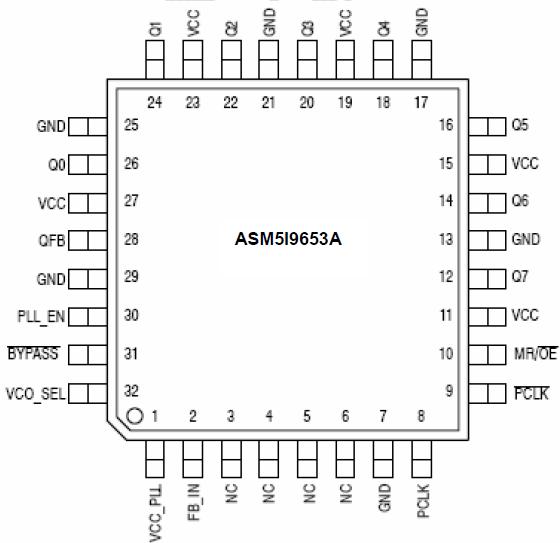
Features: 1:8 PLL based low-voltage clock generatorSupports zero-delay operation3.3V power supplyGenerates clock signals up to 125MHzPLL guaranteed to lock down to 145MHz, output frequency = 36.25MHzMaximum output skew of 150 pSDifferential LVPECL reference clock inputExternal PLL feedbackDrives u...
ASM5I9653A: Features: 1:8 PLL based low-voltage clock generatorSupports zero-delay operation3.3V power supplyGenerates clock signals up to 125MHzPLL guaranteed to lock down to 145MHz, output frequency = 36.25MH...
SeekIC Buyer Protection PLUS - newly updated for 2013!
268 Transactions
All payment methods are secure and covered by SeekIC Buyer Protection PLUS.
Features: • Low skew; low jitter PLL clock driver.• 1 to 10 differential clock distrib...
1:8 PLL based low-voltage clock generator
Supports zero-delay operation
3.3V power supply
Generates clock signals up to 125MHz
PLL guaranteed to lock down to 145MHz, output frequency = 36.25MHz
Maximum output skew of 150 pS
Differential LVPECL reference clock input
External PLL feedback
Drives up to 16 clock lines
32 lead LQFP & TQFP Packages
Ambient temperature range 0to +70
Pin and function compatible to the MPC953,MPC9653A and MPC9653
Symbol | Characteristics | Min | Max | Unit | Condition |
VCC | Supply Voltage | -0.3 | 3.9 | V | |
VIN | DC Input Voltage | -0.3 | VCC+0.3 | V | |
VOUT | DC Output Voltage | -0.3 | VCC+0.3 | V | |
IIN | DC Input Current | ±20 | mA | ||
IOUT | DC Output Current | ±50 | mA | ||
TS | Storage Temperature | -65 | 125 |
The ASM5I9653A utilizes PLL technology to frequency lock its outputs onto an input reference clock. Normal operation of it requires the connection of the QFB output to the feedback input to close the PLL feedback path (external feedback). With the PLL locked, the output frequency is equal to the reference frequency of the device and VCO_SEL selects the operating frequency range of 25 to 62.5MHz or 50 to 125MHz. The two available post-PLL dividers selected by VCO_SEL (divide-by-4 or divide-by-8) and the reference clock frequency determine the VCO frequency. Both must be selected to match the VCO frequency range. The internal VCO of the ASM5I9653A isrunning at either 4x or 8x of the reference clock frequency. The ASM5I9653A is guaranteed to lock in a low power PLL mode in the high frequency range (VCO_SEL = 0) down to PLL = 145 MHz or Fref = 36.25MHz.
The ASM5I9653A has a differential LVPECL reference input long with an external feedback input. The device is ideal for use as a zero delay, low skew fanout buffer. The device performance has been tuned and optimized for zero delay performance. The PLL_EN and BYPASS controls select the PLL bypass configuration for test and diagnosis. In ASM5I9653A configuration, the selected input reference clock is bypassing the PLL and routed either to the output dividers or directly to the outputs. The PLL bypass configurations are fully static and the minimum clock frequency
specification and all other PLL characteristics do not apply. The outputs of ASM5I9653A can be disabled (high-impedance) and the device reset by asserting the MR/OE pin. Asserting MR/OE also causes the PLL to loose lock due to missing feedback signal presence at FB_IN. Deasserting MR/OE will enable the outputs and close the phase locked loop, enabling the PLL to recover to normal operation. The ASM5I9653A is fully 3.3V compatible and requires no external loop filter components. The inputs (except PCLK) accept LVCMOS except signals while the outputs provide LVCMOS compatible levels with the capability to drive terminated 50 transmission lines. For series terminated transmission lines, each of the ASM5I9653A outputs can drive one or two traces giving the devices an effective fanout of 1:16. The device is packaged in a 7x7 mm2 32-lead LQFP & TQFP Packages.