ASM5I961P

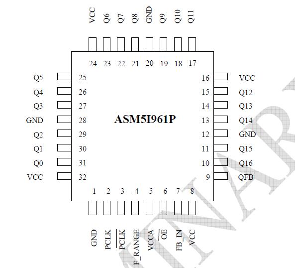
Features: 􀂃 Fully Integrated PLL􀂃 Up to 200MHz I/O Frequency􀂃 LVCMOS Outputs􀂃 Outputs Disable in High Impedance􀂃 LVPECL Reference Clock Options􀂃 LQFP Packaging􀂃 ±50pS CycleCycle Jitter􀂃 150pS Output SkewsPinoutSpecifications ...

product image

ASM5I961P Picture
SeekIC No. : 004289063 Detail

ASM5I961P: Features: 􀂃 Fully Integrated PLL􀂃 Up to 200MHz I/O Frequency􀂃 LVCMOS Outputs􀂃 Outputs Disable in High Impedance􀂃 LVPECL Reference Clock Options􀂃...

floor Price/Ceiling Price

Part Number:
ASM5I961P
Supply Ability:
5000

Price Break

  • Qty
  • 1~5000
  • Unit Price
  • Negotiable
  • Processing time
  • 15 Days
Total Cost: $ 0.00

SeekIC Buyer Protection PLUS - newly updated for 2013!

  • Escrow Protection.
  • Guaranteed refunds.
  • Secure payments.
  • Learn more >>

Month Sales

268 Transactions

Rating

evaluate  (4.8 stars)

Upload time: 2025/1/2

Payment Methods

All payment methods are secure and covered by SeekIC Buyer Protection PLUS.

Notice: When you place an order, your payment is made to SeekIC and not to your seller. SeekIC only pays the seller after confirming you have received your order. We will also never share your payment details with your seller.
Product Details

Description


Features:

􀂃 Fully Integrated PLL
􀂃 Up to 200MHz I/O Frequency
􀂃 LVCMOS Outputs
􀂃 Outputs Disable in High Impedance
􀂃 LVPECL Reference Clock Options
􀂃 LQFP Packaging
􀂃 ±50pS CycleCycle Jitter
􀂃 150pS Output Skews


Pinout

  Connection Diagram


Specifications

Symbol Parameter Min Max Unit
VCC Supply Voltage 0.3 3.6 V
VIN DC Input Voltage 0.3 VCC + 0.3 V
VOUT DC Output Voltage 0.3 VCC + 0.3 V
IIN DC Input Current ±20 mA
IOUT DC Output Current ±50 mA
TS Storage Temperature Range 40 125 °C
TDV Static Discharge Voltage
(As per JEDEC STD 22- A114-B)
2 KV


Description

The ASM5I961P is a 2.5V or 3.3V compatible, 1:18 PLL based zero delay buffer. With output frequencies of up to 200MHz, output skews of 150pS the device meets the needs of the most demanding clock tree applications.

The ASM5I961P is offered with two different input configurations. That offers an LVCMOS reference clock while it offers an LVPECL reference clock.

When pulled high the OE pin will force all of the outputs (except QFB) into a high impedance state. Because the OE pin does not affect the QFB output, down stream clocks can be disabled without the internal PLL losing lock.

The ASM5I961P is fully 2.5V or 3.3V compatible and requires no external loop filter components. All control inputs accept LVCMOS compatible levels and the outputs provide low impedance LVCMOS outputs capable of driving terminated 50 transmission lines. For series terminated lines the ASM5I961P can drive two lines per output giving the device an effective fanout of 1:36. The device is packaged in a 32 lead LQFP package to provide the optimum combination of board density and performance.


Customers Who Bought This Item Also Bought

Margin,quality,low-cost products with low minimum orders. Secure your online payments with SeekIC Buyer Protection.
Integrated Circuits (ICs)
Cables, Wires
Undefined Category
RF and RFID
Power Supplies - Board Mount
Discrete Semiconductor Products
View more