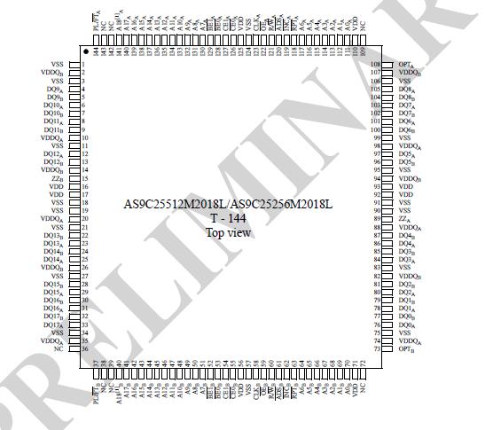
Features: • True Dual-Port memory cells that allow simultaneous access of the same memory location• Organisation: 524,288/262,144 × 18[1]• Fully Synchronous, independent operation on both ports• Selectable Pipeline or Flow-Through output mode• Fast clock speeds in Pip...
AS9C25512M2018L: Features: • True Dual-Port memory cells that allow simultaneous access of the same memory location• Organisation: 524,288/262,144 × 18[1]• Fully Synchronous, independent operation ...
SeekIC Buyer Protection PLUS - newly updated for 2013!
268 Transactions
All payment methods are secure and covered by SeekIC Buyer Protection PLUS.
Features: • True Dual-Port memory cells that allow simultaneous access of the same memory lo...
Parameter |
Symbol |
Rating |
Unit | |
Min |
Max | |||
Core supply voltage relative to VSS |
VDD |
-0.5 |
3.6 |
V |
I/O supply voltage relative to VSS |
VDDQ |
-0.3 |
3.9 |
V |
Input and I/O voltage relative to VSS |
VIN |
-0.3 |
VDDQ + 0.3 |
V |
Power Dissipation |
PD |
- |
TBD |
W |
Short circuit output current |
IOUT |
- |
TBD |
mA |
Storage Temperature |
TSTG |
-65 |
150 |
°C |
Storage Temperature under Bias |
TBIAS |
-55 |
125 |
°C |
Junction Temperature |
TJN |
- |
TBD |
°C |
device, organized as 524,288/262,144 * 18 bits. AS9C25512M2018L incorporates a selectable Flow-Through/Pipeline output feature for user flexibility. Clockto-data valid time is 2.8ns at 250 MHz for "Pipeline output" mode of operation.
Each port contains a 19/18 bit linear burst counter on the input address register that can loop through the whole address sequence. After externally loading the counter with the initial address, AS9C25512M2018L can be Incremented or Held for the next cycle. A new address can also be Loaded or the "Previous Loaded" address can be re-accessed (Repeated) using counter controls (More description to follow). The Registers of AS9C25512M2018Lon control, data, and address inputs provide minimal setup and hold times.
The memory array of AS9C25512M2018L utilizes Dual-Port memory cells to allow simultaneous access of any address from both ports. A particular port can write to a certain location while another port is reading from the same location, but the validity of read data is not guaranteed. However, the reading port is informed about the possible collision through AS9C25512M2018L collision alert signal. The result of writing to the same location by more than one port at the same time is undefined.
The Asynchronous Output Enable input pin allows asynchronous disabling of output buffers at any given time. The Byte Enable inputs of AS9C25512M2018L allow individual byte read/write operations (refer Byte Control Truth Table). An automatic power down feature, controlled by CE0 and CE1, permits the on-chip circuitry of each port to enter a very low standby power mode.
AS9C25512M2018L/AS9C25256M2018L can support an operating voltage of either 3.3V or 2.5V on either or both ports, which is controlled by the OPT pins. The power supply for the core of the device (VDD) is at 2.5V. AS9C25512M2018L is available in 256-pin Ball Grid Array (BGA), 208-pin fine pitch Ball Grid Array (fpBGA) and 144-pin Thin Quad Flatpack (TQFP)