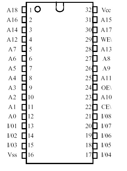
Features: • Ultra Low Power with 2V Data Retention (0.2mW MAX worst case Power-down standby)• Fully Static, No Clocks• Single +5V ±10% power supply• Easy memory expansion with CE\ and OE\ options• All inputs and outputs are TTL-compatible• Three state outputs...
AS5C4009LL: Features: • Ultra Low Power with 2V Data Retention (0.2mW MAX worst case Power-down standby)• Fully Static, No Clocks• Single +5V ±10% power supply• Easy memory expansion wit...
SeekIC Buyer Protection PLUS - newly updated for 2013!
268 Transactions
All payment methods are secure and covered by SeekIC Buyer Protection PLUS.
Features: · Access times of 15, 20 and 25 ns·Fast output enable (tAOE ) for cache applications· Lo...
• Ultra Low Power with 2V Data Retention (0.2mW MAX worst case Power-down standby)
• Fully Static, No Clocks
• Single +5V ±10% power supply
• Easy memory expansion with CE\ and OE\ options
• All inputs and outputs are TTL-compatible
• Three state outputs
• Operating temperature range: Ceramic -55oC to +125oC & -40oC to +85oC Plastic -40oC to +85oC3
1. Not applicable to plastic package
2. Applies to CW package only.
3. Contact factory for -55oC to +125oC
Voltage on Vcc Supply Relative to Vss........................-.5V to +7.0V
Voltage on any pin Relative to Vss.............................-.5V to +7.0V
Storage Temperature ........................................-65°C to +150°C
Operating Temperature Range.............................-55oC to +125oC
Soldering Temperature Range...............................................260oC
Maximum Junction Temperature**.....................................+150°C
Power Dissipation...................................................................1.0W
*Stresses greater than those listed under "Absolute Maximum Ratings" may cause permanent damage to the device. This is a stress rating only and functional operation of the device at these or any other conditions above those indicated in the operation section of this specification is not implied. Exposure to absolute maximum rating conditions for extended periods may affect reliability.
** Junction temperature depends upon package type, cycle time, loading, ambient temperature and airflow.
The AS5C4009LL is organized as 524,288 x 8 SRAM utilizing a special ultra low power design process. ASI's pinout adheres to the JEDEC standard for pinout on 4 megabit SRAMs.
The evolutionary 32 pin version allows for easy upgrades from the 1 meg SRAM design. For flexibility in memory applications, ASI AS5C4009LL offers chip enable (CE\) and output enable (OE\) capabilities.
These features of AS5C4009LL can place the outputs in High-Z for additional flexibility in system design. This devices operates from a single +5V power supply and all inputs and outputs are fully TTL-compatible. Writing to these devices is accomplished when write enable (WE\) and CE\ inputs are both LOW. Reading is accomplished when WE\ remains HIGH and CE\ and OE\ go LOW.
AS5C4009LL offers a reduced power standby mode when disabled, by lowering VCC to 2V and maintaining CE\ = 2V. This allows system designers to meet ultra low standby power requirements.