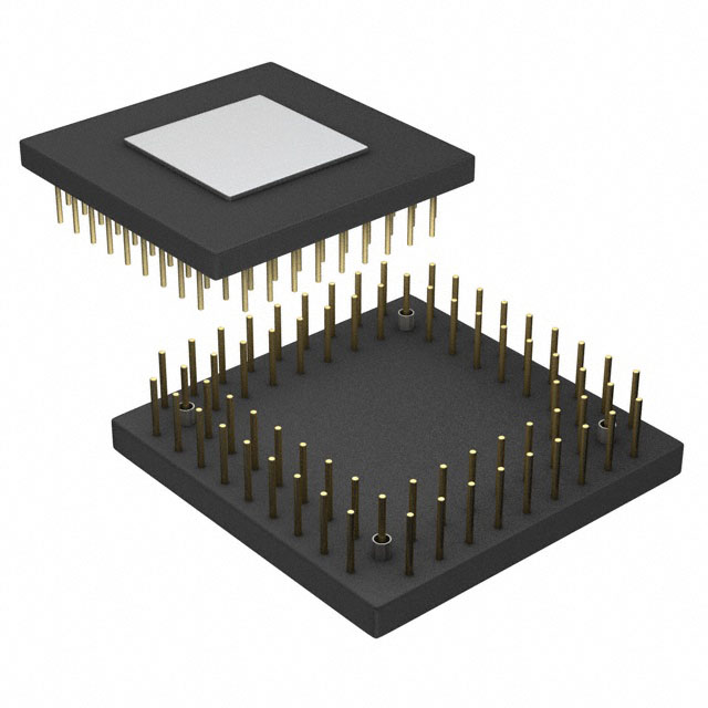
Features: • Bidirectional operation each SPORT has independent transmit and receive pins.
• Buffered (8-deep) transmit and receive ports each port has a
data register for transferring data words to and from other DSP
components and shift registers for shifting data in and out of the data registers.
• Clocking each transmit and receive port can either use an external serial
clock (fSCLK) or generate its own, in frequencies ranging
from (fSCLK/131070) Hz to (fSCLK/2) Hz.
• Word length each SPORT supports serial data words from 3 to 16 bits in
length transferred in Big Endian (MSB) or Little Endian (LSB) format.
• Framing each transmit and receive port can run with or without frame
sync signals for each data word. Frame sync signals can be generated internally
or externally, active high or low, and with either of two pulsewidths and early or late frame sync.
• Companding in hardware each SPORT can perform A-law or -law
companding according to ITU recommendation G.711. Companding can be
selected on the transmit and/or receive channel of the SPORT without additional latencies.
• DMA operations with single-cycle overhead each SPORT can automatically
receive and transmit multiple buffers of memory data, one data word each
DSP cycle. Either the DSP's core or a host processor can link or chain sequences
of DMA transfers between a SPORT and memory. The chained DMA can be
dynamically allocated and updated through the Transfer Control Blocks
(TCBs, or DMA parameters) that set up the chain.
• Interrupts each transmit and receive port generates an interrupt
upon completing the transfer of a data word or after transferring
an entire data buffer or buffers through DMA.
• Multichannel capability each SPORT supports 24 or 32 channels
and is compatible with the H.100, H.110, MVIP-90, and HMVIP standards.
Specifications
|
Parameter1 |
Absolute Maximum Rating |
| Internal (Core) Supply Voltage (VDDINT) |
0.3 V to +1.8 V |
| External (I/O) Supply Voltage (VDDEXT) |
0.3 V to +4.0 V |
| Input Voltage |
0.5 V to VDDEXT + 0.5 V |
| Output Voltage Swing |
0.5 V to VDDEXT + 0.5 V |
| Load Capacitance |
200 pF |
| Core Clock |
300 MHz |
| Peripheral Clock (SCLK) |
133 MHz |
| Storage Temperature Range |
65ºC to +150ºC |
| Lead Temperature (5 seconds) |
185ºC |
DescriptionThe ADSP21535 Blackfin DSP family assembly language instruction set employs an algebraic syntax that was designed for ease of coding and readability. The instructions have been specifically tuned to provide a flexible, densely encoded instruction set that compiles to a very small final memory size. The instruction set also provides fully featured multifunction instructions that allow the programmer to use many of the DSP core resources in a single instruction. Coupled with many features more often seen on microcontrollers, this instruction set is very efficient when compiling C and C++ source code. In addition, the architecture supports both a user (algorithm/application code) and a supervisor (O/S kernel, device drivers, debuggers, ISRs) mode of operations, allowing multiple levels of access to core DSP resources of ADSP21535.

 ADSP21535 Data Sheet


