Features: 6.25 ns Instruction Cycle Time (Internal), for up to
160 MIPS Sustained Performance
ADSP-218x Family Code Compatible with the Same
Easy -to-Use Algebraic Syntax
Single-Cycle Instruction Execution
Up to 16M words of Addressable Memory Space with
24 Bits of Addressing Width
Dual Purpose Program Memory for Both Instruction and
Data Storage
Fully Transparent Instruction Cache Allows Dual
Operand Fetches in Every Instruction Cycle
Unified Memory Space Permits Flexible Address
Generation, Using Two Independent DAG Units
Independent ALU, Multiplier/Accumulator, and Barrel
Shifter Computational Units with Dual 40-bit
Accumulators
Single-Cycle Context Switch between Two Sets of
Computational and DAG Registers
Parallel Execution of Computation and Memory
Instructions
Pipelined Architecture Supports Efficient Code
Execution at Speeds up to 160 MIPS
Register File Computations with All Nonconditional,
Nonparallel Computational Instructions
Powerful Program Sequencer Provides Zero-Overhead
Looping and Conditional Instruction Execution
Architectural Enhancements for Compiled C
Code Efficiency
ADSP-2196 DSP FEATURES
16K Words of On-Chip RAM, Configured as 8K Words
On-Chip 24-bit RAM and 8K Words On-Chip 16-bit RAM
16K Words of On-Chip 24-bit ROM
Architecture Enhancements beyond ADSP-218x Family
are Supported with Instruction Set Extensions for
Added Registers, Ports, and Peripherals
Flexible Power Management with Selectable
Power-Down and Idle Modes
Programmable PLL Supports 1� to 32� Frequency
Multiplication, Enabling Full-Speed Operation from
Low-Speed Input Clocks
2.5 V Internal Operation Supports 3.3 V Compliant I/O
Three Full-Duplex Multichannel Serial Ports, Each
Supporting H.100 Standard with A-Law and �-Law
Companding in Hardware
Two SPI-Compatible Ports with DMA Capability
One UART Port with DMA Capability
16 General-Purpose I/O Pins (Eight Dedicated/Eight
Programmable from the External Memory Interface)
with Integrated Interrupt Support
Three Programmable 32-Bit Interval Timers with
Pulsewidth Counter, PWM Generation, and Externally
Clocked Timer Capabilities
Up to 11 DMA Channels can be Active at any Given Time
Host Port With DMA Capability for Efficient, Glueless Host
Interface (16-Bit Transfers)
External Memory Interface Features Include:
Direct Access from the DSP to External Memory for
Data and Instructions.
Support for DMA Block Transfers to/from
External Memory.
Separate Peripheral Memory Space with Parallel
Support for 224K External 16-Bit Registers.
Four General-Purpose Memory Select Signals that
Provide Access to Separate Banks of External
Memory. Bank Boundaries and Size Are User-
Programmable.
Programmable Waitstate Logic with ACK Signal and
Separate Read and Write Wait Counts. Wait Mode
Completion Supports All Combinations of ACK
and/or Wait Count.
I/O Clock Rate Can Be Set to the Peripheral Clock Rate
Divided by 1, 2, 4, 16, or 32 to Allow Interface to Slow
Memory Devices.
Address Translation and Data Word Packing is Provided
to Support an 8- or 16-Bit External Data Bus.
Programmable Read and Write Strobe Polarity.
Separate Configuration Registers for the Four
General-Purpose, Peripheral, and Boot
Memory Spaces.
Bus Request and Grant Signals Support the Use of the
External Bus by an External Device.
Boot Methods Include Booting Through External Memory
Interface, SPI Ports, UART Port, or Host Interface
IEEE JTAG Standard 1149.1 Test Access Port Supports
On-Chip Emulation and System Debugging
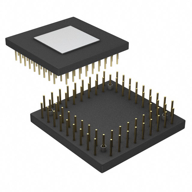
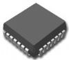
144-Lead LQFP Package (20× 20 × 1.4 mm) and 144-Lead
Mini-BGA Package (10 × 10 × 1.25 mm)SpecificationsVDDINTInternal (Core) Supply Voltage1,2 ...0.3 to 3.0 V
VDDEXTExternal (I/O) Supply Voltage .........0.3 to 4.6 V
VILVIHInput Voltage ..................0.5 to VDDEXT+0.5 V
VOLVOHOutput Voltage Swing ...0.5 to VDDEXT+0.5 V
CLLoad Capacitance............................................ 200 pF
tCCLKCore Clock Period........................................6.25 ns
fCCLKCore Clock Frequency.............................. 160 MHz
tHCLKPeripheral Clock Period..................................10 ns
fHCLKPeripheral Clock Frequency...................... 100 MHz
TSTOREStorage Temperature Range .......... 65 to 150
TLEADLead Temperature (5 seconds)...................... 185DescriptionThe ADSP-2196 DSP is a single-chip microcomputer optimized for digital signal processing (DSP) and other high speed numeric processing applications.
The ADSP-2196 combines the ADSP-219x family base architecture (three computational units, two data address generators, and a program sequencer) with three serial ports, two SPI-compatible ports, one UART port, a DMA controller, three programmable timers, general-purpose Programmable Flag pins, extensive interrupt capabilities, and on-chip program and data memory spaces.
The ADSP-2196 architecture is code-compatible with ADSP-218x family DSPs. Although the architectures are compatible, the ADSP-2196 architecture has a number of enhancements over the ADSP-218x architecture. The enhancements to computational units, data address generators,and program sequencer make it more flexible and even easier to program than the ADSP-218x DSPs.
Indirect addressing options provide addressing flexibility-premodify with no update, pre- and post-modify by an immediate 8-bit, two's-complement value and base address registers for easier implementation of circular buffering.
The ADSP-2196 integrates 32K words of on-chip memory configured as 8K words (24-bit) of program RAM, 8K words (16-bit) of data RAM, and 16K words (24-bit) of program ROM. Power-down circuitry is also provided to meet the low power needs of battery-operated portable equipment. The ADSP-2196 is available in 144-lead LQFP and mini-BGA packages.
Fabricated in a high-speed, low-power, CMOS process, the ADSP-2196 operates with a 6.25 ns instruction cycle time (160MIPS). All instructions, except two multiword instructions, can execute in a single DSP cycle.
The ADSP-2196's flexible architecture and comprehensive instruction set support multiple operations in parallel. For example, in one processor cycle,it can:
• Generate an address for the next instruction fetch
• Fetch the next instruction
• Perform one or two data moves
• Update one or two data address pointers
• Perform a computational operation
These operations take place while the processor continues to:
• Receive and transmit data through two serial ports
• Receive and/or transmit data from a Host
• Receive or transmit data through the UART
• Receive or transmit data over two SPI ports
• Access external memory through the external memory interface
• Decrement the timers

 ADSP-2196 Data Sheet