Application` 13.3 ns Instruction Cycle Time @ 2.5 Volts (Internal), 75 MIPS Sustained Performance
` Single-Cycle Instruction Execution
` Single-Cycle Context Switch
` 3-Bus Architecture Allows Dual Operand Fetches in Every Instruction Cycle
` Multifunction Instructions
` Power-Down Mode Featuring Low CMOS Standby
Power Dissipation with 200 CLKIN Cycle Recovery from Power-Down Condition
` Low Power Dissipation in Idle Mode
` ADSP-2100 Family Code Compatible (Easy to Use AlgebraicSyntax), with Instruction Set Extensions
` 192K Bytes of On-Chip RAM, Configured as 32K Words
On-Chip Program Memory RAM and 48K Words On-Chip Data Memory RAM
` Dual Purpose Program Memory for Both Instruction and Data Storage
` Independent ALU, Multiplier/Accumulator and Barrel
Shifter Computational Units
` Two Independent Data Address Generators
` Powerful Program Sequencer Provides Zero Overhead
Looping Conditional Instruction Execution
` Programmable 16-Bit Interval Timer with Prescaler
` 100-Lead LQFP` Flexible I/O Structure Allows 2.5 V or 3.3 V Operation;
All Inputs Tolerate Up to 3.6 V, Regardless of Mode
` 16-Bit Internal DMA Port for High Speed Access to On-Chip Memory (Mode Selectable)
` 4 MByte Memory Interface for Storage of Data Tables and Program Overlays (Mode Selectable)
` 8-Bit DMA to Byte Memory for Transparent Program and Data Memory Transfers (Mode Selectable)
` I/O Memory Interface with 2048 Locations Supports
Parallel Peripherals (Mode Selectable)
` Programmable Memory Strobe and Separate I/O
Memory Space Permits "Glueless" System Design
` Programmable Wait-State Generation
` Two Double-Buffered Serial Ports with Companding
Hardware and Automatic Data Buffering
` Automatic Booting of On-Chip Program Memory from
Byte-Wide External Memory, e.g., EPROM, orThrough Internal DMA Port
` Six External Interrupts
` 13 Programmable Flag Pins Provide Flexible System Signaling
` UART Emulation through Software SPORT Reconfiguration
` ICE-Port™ Emulator Interface Supports Debugging in Final Systems
Pinout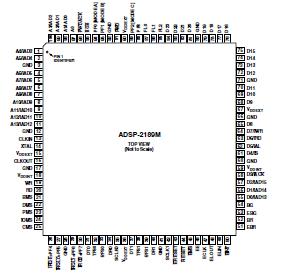 Specifications
| Parameter |
Value |
|
Min |
Max |
Internal Supply Voltage (VDDINT)
External Supply Voltage (VDDEXT)
Input Voltage2
Output Voltage3 Swing3
Operating Temperature Range (Ambient)
Storage Temperature Range
Lead Temperature (5 sec) LQFP |
0.3 V
0.3 V
0.5 V
0.5 V
40°C
65°C |
+3.0 V
+4.6 V
+4.6 V
VDDEXT + 0.5 V
+85°C
+150°C
+280°C |
NOTES
1Stresses above those listed under Absolute Maximum Ratings may cause permanent damage to the device. These are stress ratings only; functional operation of the device at these or any other conditions above those indicated in the operational sections of this specification is not implied. Exposure to absolute maximum rating conditions for extended periods may affect device reliability.
2Applies to Bidirectional pins (D0D23, RFS0, RFS1, SCLK0, SCLK1, TFS0,TFS1, A1A13, PF0PF7) and Input only pins (CLKIN, RESET, BR, DR0,DR1, PWD).
3Applies to Output pins (BG, PMS, DMS, BMS, IOMS, CMS,RD, WR, PWDACK,A0, DT0, DT1, CLKOUT, FL2-0, BGH).DescriptionThe ADSP-2189M is a single-chip microcomputer optimized for digital signal processing (DSP) and other high speed numeric processing applications.
The ADSP-2189M combines the ADSP-2100 family base architecture (three computational units, data address generators and a program sequencer) with two serial ports, a 16-bit internal DMA port, a byte DMA port, a programmable timer, Flag I/O,extensive interrupt capabilities, and on-chip program and data memory.
The ADSP-2189M integrates 192K bytes of on-chip memory configured as 32K words (24-bit) of program RAM and 48K words (16-bit) of data RAM. Power-down circuitry is also provided to meet the low power needs of battery operated portable equipment. The ADSP-2189M is available in a 100-lead LQFP package.
In addition, the ADSP-2189M supports new instructions, which include bit manipulations-bit set, bit clear, bit toggle, bit test-new ALU constants, new multiplication instruction (x squared), biased rounding, result free ALU operations, I/O memory transfers and global interrupt masking, for increased flexibility.
Fabricated in a high speed, low power, CMOS process, the ADSP-2189M operates with a 13.3 ns instruction cycle time. Every instruction can execute in a single processor cycle.
The ADSP-2189M's flexible architecture and comprehensive instruction set allow the processor to perform multiple operations in parallel. In one processor cycle:
• Generate the next program address
• Fetch the next instruction
• Perform one or two data moves
• Update one or two data address pointers
• Perform a computational operation
This takes place while the processor continues to:
• Receive and transmit data through the two serial ports
• Receive and/or transmit data through the internal DMA port
• Receive and/or transmit data through the byte DMA port
• Decrement timer

 ADSP-2189M Data Sheet