Features: 30 ns Instruction Cycle Time (33 MIPS) from
16.67 MHz Crystal at 5.0 V
50 ns Instruction Cycle Time (20 MIPS) from 10 MHz
Crystal at 3.3 V
ADSP-2100 Family Code & Function Compatible with
New Instruction Set Enhancements for Bit Manipula-
tion Instructions, Multiplication Instructions, Biased
Rounding, and Global Interrupt Masking
Bus Grant Hang Logic
2K Words of On-Chip Program Memory RAM
2K Words of On-Chip Data Memory RAM
8K Words of On-Chip Program Memory ROM
(ADSP-2172)
8- or 16-Bit Parallel Host Interface Port
300 mW Typical Power Dissipation at 5.0 V at 30 ns
70 mW Typical Power Dissipation at 3.3 V at 50 ns
Powerdown Mode Featuring Less than 0.55 mW (ADSP-
2171/ADSP-2172) or 0.36 mW (ADSP-2173) CMOS
Standby Power Dissipation with 100 Cycle Recovery
from Powerdown
Dual Purpose Program Memory for Both Instruction
and Data Storage
Independent ALU, Multiplier/Accumulator, and Barrel
Shifter Computational Units
Two Independent Data Address Generators
Powerful Program Sequencer Provides
Zero Overhead Looping
Conditional Instruction Execution
Two Double-Buffered Serial Ports with Companding
Hardware and Automatic Data Buffering
Programmable 16-Bit Interval Timer with Prescaler
Programmable Wait State Generation
Automatic Booting of Internal Program Memory from
Byte-Wide External Memory, e.g., EPROM, or
Through Host Interface Port
Stand-Alone ROM Execution (Optional)
Single-Cycle Instruction Execution
Single-Cycle Context Switch
Multifunction Instructions
Three Edge- or Level-Sensitive External Interrupts
Low Power Dissipation in Standby Mode
128-Lead TQFP and 128-Lead PQFPPinout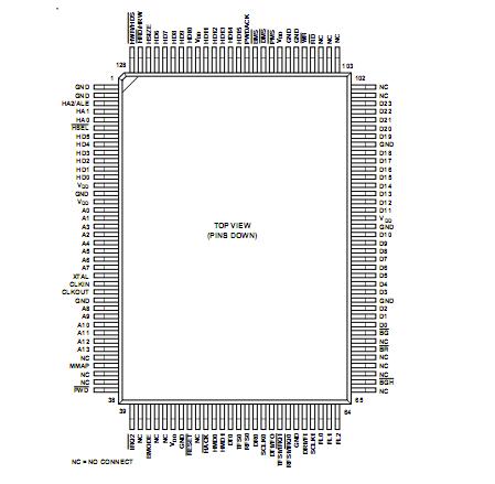 Specifications
Supply Voltage . . . . . . . . . . . . . . . . . . . . . . . . . . 0.3 V to +7 V
Input Voltage . . . . . . . . . . . . . . . . . . . . . 0.3 V to VDD + 0.3 V
Output Voltage Swing . . . . . . . . . . . . . . 0.3 V to VDD + 0.3 V
Operating Temperature Range (Ambient) . . . . 40°C to +85°C
Storage Temperature Range . . . . . . . . . . . . .65°C to +150°C
Lead Temperature (5 sec) TQFP . . . . . . . . . . . . . . . . +280°C
Lead Temperature (5 sec) PQFP . . . . . . . . . . . . . . . . . +280°C
*
Stresses above those listed under "Absolute Maximum Ratings" may cause permanent damage to the device. These are stress ratings only, and functional operation of the device at these or any other conditions above those indicated in the operational sections of this specification is not implied. Exposure to absolute maximum rating conditions for extended periods may affect device reliability.
DescriptionThe ADSP-217x are single-chip microcomputers optimized for digital signal processing (DSP) and other high-speed numeric processing applications. The ADSP-2171 and ADSP-2172 are designed for 5.0 V applications. The ADSP-2173 is designed for 3.3 V applications. The ADSP-2172 also has 8K words (24-bit) of program ROM.
The ADSP-217x combines the ADSP-2100 base architecture (three computational units, data address generators, and a program sequencer) with two serial ports, a host interface port, a programmable timer, extensive interrupt capabilities, and onchip program and data memory.
In addition, the ADSP-217x supports new instructions, which include bit manipulationsbit set, bit clear, bit toggle, bit testnew ALU constants, new multiplication instruction (x squared), biased rounding, and global interrupt masking, for increased flexibility. The ADSP-217x also has a Bus Grant Hang Logic (BGH) feature.
The ADSP-217x provides 2K words (24-bit) of program RAM and 2K words (16-bit) of data memory. The ADSP-2172 provides an additional 8K words (24-bit) of program ROM. Powerdown circuitry is also provided to meet the low power needs of battery operated portable equipment. The ADSP-217x is available in 128-pin TQFP and 128-pin PQFP packages.
Fabricated in a high-speed, double metal, low power, CMOS process, the ADSP-217X operates with a 30 ns instruction cycle time. Every instruction can execute in a single processor cycle. The ADSP-217x's flexible architecture and comprehensive instruction set allow the processor to perform multiple operations in parallel. In one processor cycle the ADSP-217x can:
• generate the next program address
• fetch the next instruction
• perform one or two data moves
• update one or two data address pointers
• perform a computational operation
This takes place while the processor continues to:
• receive and transmit data through the two serial ports
• receive and/or transmit data through the host interface port
• decrement timer

 ADSP-2171 Data Sheet