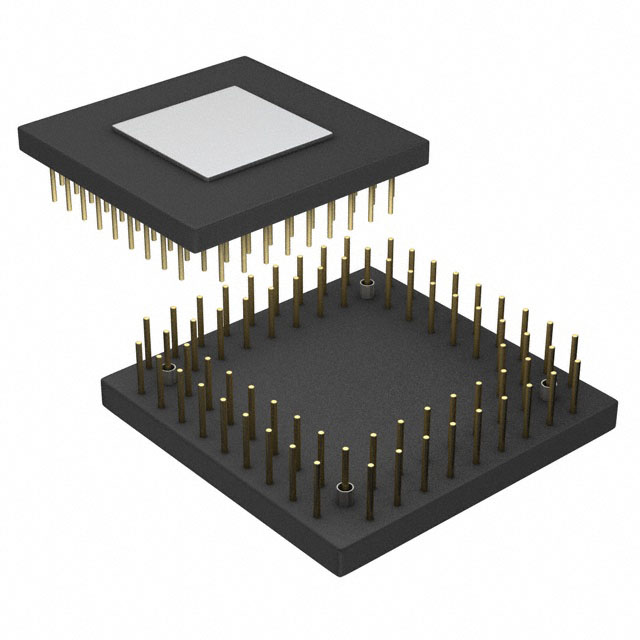
Features: • Two processing elements, each of which comprises an ALU, Multiplier, Shifter and Data Register File
• Data Address Generators (DAG1, DAG2)
• Program sequencer with instruction cache
• PM and DM buses capable of supporting four 32-bit data transfers between memory and the core at every core processor cycle
• Three Programmable Interval Timers with PWM Generation, PWM Capture/Pulse width Measurement, and External Event Counter Capabilities
• On-Chip SRAM (2 Mbits)
• On-Chip dual-ported, mask-programmable ROM (4 Mbits)
• 8- or 16-bit Parallel port that supports interfaces to off-chip memory peripherals
• DMA controller
• Six serial ports
• SPI-compatible interface
• Digital Audio Interface that includes a precision clock generator (PCG), an input data port (IDP), 6 serial ports, 8 serial interfaces, a 20-bit parallel input port, 10 interrupts, 6 flag outputs, 6 flag inputs, 3 timers, and a flexible signal routing unit (SRU)
• JTAG test access port
SpecificationsInternal (Core) Supply Voltage (VDDINT)1 ...........0.3 V to +1.5 V
Analog (PLL) Supply Voltage (AVDD)1 .................-0.3 V to +1.5 V
External (I/O) Supply Voltage (VDDEXT)1 ...........-0.3 V to +4.6 V
Input Voltage ....................................-0.5 V to VDDEXT 1 + 0.5 V
Output Voltage Swing .......................-0.5 V to VDDEXT 1 + 0.5 V
Load Capacitance1 ...........................................................200 pF
Storage Temperature Range1 ..........................-65°C to +150°C
1)Stresses greater than those listed above may cause permanent damage to the device. These are stress ratings only, and functional operation of the device at these or any other conditions greater than those indicated in the operational sections of this specification is not implied. Exposure to absolute maximum rating conditions for extended periods may affect device reliability.
DescriptionThe ADSP-21266 SHARC DSP is a member of the SIMD SHARC family of DSPs featuring Analog Devices' Super Harvard Architecture. The ADSP-21266 is source code compatible with the ADSP-21160 and ADSP-21161 DSPs as well as with first generation ADSP-2106x SHARC processors in SISD (Single-Instruction, Single-Data) mode. Like other SHARC DSPs, the product is a 32-bit processor optimized for high performance audio applications. It is available in a 200 MHz or a 150 MHz core, dual-ported on-chip SRAM and mask-programmable ROM, multiple internal buses to eliminate I/O bottlenecks, and an innovative Digital Audio Interface (DAI).
The ADSP-21266 offers a Single-Instruction Multiple-Data (SIMD) architecture, which was first introduced with the ADSP- 21160 and ADSP-21161. As shown in the Functional Block Diagram on page 1, it uses two computational units to deliver a 5 to 10 times performance increase over the ADSP-2106x on a range of DSP algorithms. Fabricated in a state-of-the-art, high speed, low power CMOS process, the ADSP-21266 DSP achieves an instruction cycle time of 5 ns at 200 MHz or 6.6 ns at150 MHz. With its SIMD computational hardware, the ADSP-21266 can perform 1200 MFLOPS running at 200 MHz, or 900 MFLOPS running at150 MHz.

 ADSP-21266 Data Sheet


