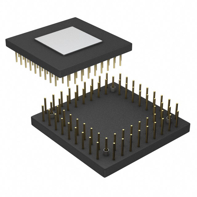
Features: · Superscalar IEEE Floating-Point Processor· Off-Chip Harvard Architecture Maximizes Signal· Processing Performance· 30 ns, 33.3 MIPS Instruction Rate, Single-Cycle· Execution· 100 MFLOPS Peak, 66 MFLOPS Sustained Performance· 1024-Point Complex FFT Benchmark: 0.58 ms· Divide (y/x): 180 ...
ADSP-2102: Features: · Superscalar IEEE Floating-Point Processor· Off-Chip Harvard Architecture Maximizes Signal· Processing Performance· 30 ns, 33.3 MIPS Instruction Rate, Single-Cycle· Execution· 100 MFLOPS ...
SeekIC Buyer Protection PLUS - newly updated for 2013!
268 Transactions
All payment methods are secure and covered by SeekIC Buyer Protection PLUS.
The ADSP-21020 is the first member of Analog Devices' family of single-chip IEEE floating-point processors optimized for digital signal processing applications. Its architecture is similar to that of Analog Devices' ADSP-2100 family of fixed-point DSP processors.
Fabricated in a high-speed, low-power CMOS process, the ADSP-21020 has a 30 ns instruction cycle time. With a highperformance on-chip instruction cache, the ADSP-21020 can execute every instruction in a single cycle. The ADSP-21020 features:
• Independent Parallel Computation Units
The arithmetic/logic unit (ALU), multiplier and shifter perform single-cycle instructions. ADSP-2102 is architecturally arranged in parallel, maximizing computational throughput. A single multifunction instruction executes parallel ALU andmultiplier operations. These computation units support IEEE 32-bit single-precision floating-point, extended precision 40-bit floating-point, and 32-bit fixed-point data formats.
• Data Register File
A general-purpose data register file is used for transferring data between the computation units and the data buses, and for storing intermediate results. This 10-port (16-register) register file, combined with the ADSP-21020's Harvard architecture, allows unconstrained data flow between computation units and off-chip memory.
• Single-Cycle Fetch of Instruction and Two Operands The ADSP-21020 uses a modified Harvard architecture in which data memory stores data and program memory stores both instructions and data. Because of its separate program and data memory buses and on-chip instruction cache, the processor can simultaneously fetch an operand from data memory, an operand from program memory, and an instruction from the cache, all in a single cycle.
• Memory Interface
Addressing of external memory devices by the ADSP-21020 is facilitated by on-chip decoding of high-order address lines to generate memory bank select signals. Separate control lines are also generated for simplified addressing of page-mode DRAM.
The ADSP-21020 provides programmable memory wait states, and external memory acknowledge controls allow interfacing to peripheral devices with variable access times.