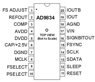
Features: +2.3 V to +5.5 V Power Supply
50 MHz Speed
Low Jitter Clock Output
Sine Output/Triangular Output
Serial Loading
Power-Down Option
Narrowband SFDR > 72 dB
20 mW Power Consumption at 3 V
20-Pin TSSOPApplicationTest Equipment
Slow Sweep Generator
DDS Tuning
Digital ModulationPinout Specifications
(TA = +25°C unless otherwise noted)
AVDD to AGND . . . . . . . . . . . . . . . . . . . .. . .0.3 V to +6 V
DVDD to DGND . . . . . . . . . . . . . . . . . . . .. . .0.3 V to +6 V
AVDD to DVDD . . . . . . . . . . . . . . . . . . . . 0.3 V to +0.3 V
AGND to DGND. . . . . . . . . . . . . . . . . . . . 0.3 V to +0.3 V
CAP/2.5V . . . . . . . . . . . . . . . . . . . . . . . . . . . . . . . . . .2.75 V
Digital I/O Voltage to DGND . . .. . ..0.3 V to DVDD + 0.3 V
Analog I/O Voltage to AGND . . .. . .0.3 V to AVDD + 0.3 V
Operating Temperature Range
Industrial (B Version) . . . . . . . . . . . . 40°C to +85°C
Storage Temperature Range . . . . . . 65°C to +150°C
Maximum Junction Temperature . . . . . . . . . . . . +150°C
TSSOP Package
JA Thermal Impedance . . . . . . . . . . . . . . . . . . .143°C/W
JC Thermal Impedance . . . . . . . . . . . . . . . . . . .45°C/W
Lead Temperature, Soldering (10 sec) . . . . . . . .300°C
IR Reflow, Peak Temperature . . . . . . . . . . . . . . . 220°C
DescriptionThe AD9834 is a numerically controlled oscillator employing a phase accumulator, a SIN ROM and a 10-bit D/A converter integrated on a single CMOS chip. Clock rates up to 50 MHz are supported with a power supply from 2.3 V to 5.5 V.Capability for phase modulation and frequency modula-tion is provided. Frequency accuracy can be controlled to one part in 0.25 billion. Modulation is effected by loading registers through the serial interface.
The AD9834 offers the user a variety of output waveforms. The SIN ROM can be bypassed so that a linear up/down ramp is output from the DAC. If the SINn ROM is not by-passed, a sinusoidal output is available. Also, if a clock output is required, the MSB of the DAC data can be output, or the on-chip comparator can be used.
The digital section is driven by an on-board regulator which steps down the applied DVDD to +2.5 V when DVDD exceeds +2.5 V. The analog and digital sections are independent and can be run from different power supplies e.g. AVDD can equals 5 V with DVDD equal to 3 V, etc.
The AD9834 has a power-down pin (SLEEP) which allows external control of a power-down mode. Sections of the device which are not being used can be powered down to minimise the current consumption e.g. the DAC can be powered down when a clock output is being generated. The part is available in a 20-pin TSSOP package.

 AD9834 Data Sheet


