Features: Member of Pin-Compatible TxDAC Product Family
125 MSPS Update Rate
8-Bit Resolution
Linearity: 1/4 LSB DNL
1/4 LSB INL
Differential Current Outputs
SINAD @ 5 MHz Output:50 dB
Power Dissipation:175 mW @ 5V to 45mW @ 3V
Power-Down Mode:20 mW @ 5V
On-Chip 1.20 V Reference
Single +5 V or +3 V Supply Operation
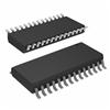
Packages:28-Lead SOIC and 28-Lead TSSOP
Edge-Triggered Latches
Fast Settling: 35 ns Full-Scale Settling to 0.1%ApplicationCommunications
Signal Reconstruction
InstrumentationPinout SpecificationsParameter With Respect to Min Max Units
AVDD ACOM 0.3 +6.5 V
DVDD DCOM 0.3 +6.5 V
ACOM DCOM 0.3 +0.3 V
AVDD DVDD 6.5 +6.5 V
CLOCK, SLEEP DCOM 0.3 DVDD + 0.3 V
Digital Inputs DCOM 0.3 DVDD + 0.3 V
IOUTA, IOUTB ACOM 1.0 AVDD + 0.3 V
COMP1, COMP2 ACOM 0.3 AVDD + 0.3 V
REFIO, FSADJ ACOM 0.3 AVDD + 0.3 V
REFLO ACOM 0.3 +0.3 V
Junction Temperature +150 °C
Storage Temperature 65 +150 °C
Lead Temperature
(10 sec) +300 °CDescriptionThe AD9708 is the 8-bit resolution member of the TxDAC series of high performance, low power CMOS digital-to analog converters (DACs). The TxDAC family, which consists of pin compatible 8-, 10-, 12-, and 14-bit DACs, was specifically opti- mized for the transmit signal path of communication systems. All of the devices share the same interface options, small outline package and pinout, thus providing an upward or downward component selection path based on performance, resolution and cost. The AD9708 offers exceptional ac and dc performance while supporting update rates up to 125 MSPS.
The AD9708°Os flexible single-supply operating range of +2.7 to +5.5 V and low power dissipation are well suited for portable and low power applications. Its power dissipation can be further reduced to 45 mW, without a significant degradation in performance, by lowering the full-scale current output. In addi-tion, a power-down mode reduces the standby power dissipa-tion to approximately 20 mW.
The AD9708 is manufactured on an advanced CMOS process. A segmented current source architecture is combined with a proprietary switching technique to reduce spurious components and enhance dynamic performance. Edge-triggered input latches and a temperature compensated bandgap reference have been inte-grated to provide a complete monolithic DAC solution. Flexible supply options support +3 V and +5 V CMOS logic families.
The AD9708 is a current-output DAC with a nominal full-scale output current of 20 mA and > 100 k output impedance.
Differential current outputs of AD9708 are provided to support single-ended or differential applications. The current outputs may be directly tied to an output resistor to provide two complemen-tary, single-ended voltage outputs. The output voltage compliance range is 1.25V.
The AD9708 contains a 1.2 V on-chip reference and reference control amplifier, which allows the full-scale output current to be simply set by a single resistor. The AD9708 can be driven by a variety of external reference voltages. The AD9708's full-scal current can be adjusted over a 2mA to 20 mA range without any degradation in dynamic performance. Thus, the AD9708 may operate at reduced power levels or be adjusted over a 20dB range to provide additional gain ranging capabilities.
The AD9708 is available in 28-lead SOIC and 28-lead TSSOP packages. It is specified for operation over the industrial tem-perature range.

 AD9708* Data Sheet