Features: Micropower: 100 mA/DAC
0.1 mA Typical Power Shutdown
Single Supply +2.7 V to +5.5 V Operation
Compact 1.1 mm Height TSSOP 24-Lead Package
AD7396: 12-Bit Resolution
AD7397: 10-Bit Resolution
0.9 LSB Differential Nonlinearity ErrorApplication-Automotive Output Span Voltage
-Portable Communications
-Digitally Controlled Calibration
-PC PeripheralsPinout Specifications
| Resolution (Bits) |
10bit |
| DAC Update Rate |
17kSPS |
| DAC Settling Time |
60s |
| # DAC Outputs |
2 |
| DAC Type |
Voltage Out |
| DAC Input Format |
Par |
| Output FSR |
(Uni Vref) |
| Ref Int/Ext |
Ext |
| Supply Vnom |
Single(+3),Single(+3.3),Single(+5) |
| Pwr Diss |
1mW |
| Package |
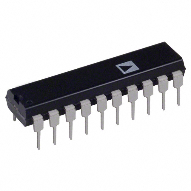
DIP,SOIC,SOP |
VDDto GND . . . . . . . . . . . . . . . . . . . . . . . . . . . .0.3 V, +8 V
VREFto GND . . . . . . . . . . . . . . . . . . . . . . . . . . .0.3 V, VDD
Logic Inputs to GND . . . . . . . . . . . . . . . . . . . . .0.3 V, +8 V
VOUTto GND . . . . . . . . . . . . . . . . . . . . .0.3 V, VDD+ 0.3 V
AGND to DGND . . . . . . . . . . . . . . . . . . . . . .. . .0.3 V, +2 V
IOUTShort Circuit to GND . . . . . . . . . . . .. . . . . . . . .+50 mA
Package Power Dissipation . . . . . . . . . . . .(TJmax TA)/JA
Thermal Resistance JA
24-Lead Plastic DIP Package (N-24) . . . . . . . . . .+63°C/W
24-Lead SOIC Package (R-24) . . . . . . . . . . . . . . .+70°C/W
24-Lead Thin Shrink Surface Mount (RU-24) . ..+143°C/W
Maximum Junction Temperature (TJmax) . . . . . . . . .+150°C
Operating Temperature Range . . . . . . . . .40°C to +85°C
AD7397AN, AD7397AR Only . . . . . . ... .40°C to +125°C
Storage Temperature Range . . . . . . . . ..65°C to +150°C
Lead Temperature
N-24 (Soldering, 10 sec) . . . . . . . . . . . . . . . . . . . . . .+300°C
R-24 (Vapor Phase, 60 sec) . . . . . . . . . . . . . . . . . . .+215°C
RU-24 (Infrared, 15 sec) . . . . . . . . . . . . . . . . . . . . . .+224°CDescriptionThe AD7396/AD7397 series of dual, 12-bit and 10-bit voltage-output digital-to-analog converters are designed to operate from a single +3 V supply. Built using a CBCMOS process, these monolithic DACs offer the user low cost and ease of use in single supply +3 V systems. Operation is guaranteed over the
supply voltage range of +2.7 V to +5.5 V, making this device ideal for battery operated applications.
A 12-bit wide data latch loads with a 45 ns write time allowing interface to fast processors without wait states. The double buffered input structure allows the user to load the input registers one at a time, then a single load strobe tied to both LDA</a>+LDB</a> inputs will simultaneously update both DAC out-puts. LDA</a>and LDB</a>can also be independently activated to immediately update their respective DAC registers. An address input (A/B) decodes DACA or DACB when the chip select CS</a> input is strobed. Additionally, an asynchronous RS</a>input sets the output to zero-scale at power on or upon user demand. Power shutdown to submicroamp levels is directly controlled by the active low SHDN</a>pin. While in the power shutdown state register data can still be changed even though the output buffer is in an open circuit state. Upon return to the normal operating state the latest data loaded in the DAC register will establish the output voltage.
Both parts are offered in the same pinout, allowing users to select the amount of resolution appropriate for their applications without circuit card changes.
The AD7396/AD7397 are specified for operation over the ex-tended industrial (40°C to +85°C) temperature range. The AD7397AR is specified for the 40°C to +125°C automotive temperature range. AD7396/AD7397s are available in plastic DIP, and 24-lead SOIC packages. The AD7397ARU is avail-
able for ultracompact applications in a thin 1.1 mm height TSSOP 24-lead package.

 AD7397 Data Sheet


