AD7395

Features: Micropower: 100 A/DAC0.1 A Typical Power ShutdownSingle-Supply +2.7 V to +5.5 V OperationCompact 1.1 mm Height TSSOP-14 PackageAD7394/12-Bit ResolutionAD7395/10-Bit ResolutionSerial Interface with Schmitt Trigger InputsAPPLICATIONSAutomotive Output Span VoltagePortable CommunicationsDigi...

product image

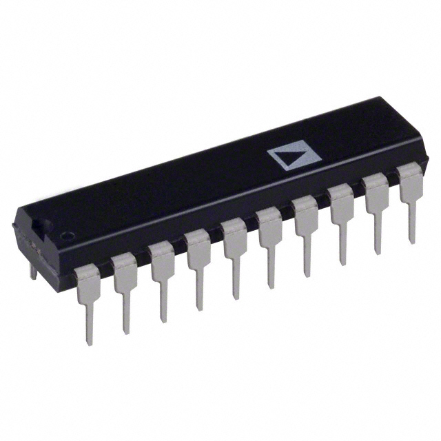
AD7395 Picture
SeekIC No. : 004270120 Detail

AD7395: Features: Micropower: 100 A/DAC0.1 A Typical Power ShutdownSingle-Supply +2.7 V to +5.5 V OperationCompact 1.1 mm Height TSSOP-14 PackageAD7394/12-Bit ResolutionAD7395/10-Bit ResolutionSerial Interf...

floor Price/Ceiling Price

Part Number:
AD7395
Supply Ability:
5000

Price Break

  • Qty
  • 1~5000
  • Unit Price
  • Negotiable
  • Processing time
  • 15 Days
Total Cost: $ 0.00

SeekIC Buyer Protection PLUS - newly updated for 2013!

  • Escrow Protection.
  • Guaranteed refunds.
  • Secure payments.
  • Learn more >>

Month Sales

268 Transactions

Rating

evaluate  (4.8 stars)

Upload time: 2025/1/2

Payment Methods

All payment methods are secure and covered by SeekIC Buyer Protection PLUS.

Notice: When you place an order, your payment is made to SeekIC and not to your seller. SeekIC only pays the seller after confirming you have received your order. We will also never share your payment details with your seller.
Product Details

Description


Features:

Micropower: 100 A/DAC
0.1 A Typical Power Shutdown
Single-Supply +2.7 V to +5.5 V Operation
Compact 1.1 mm Height TSSOP-14 Package
AD7394/12-Bit Resolution
AD7395/10-Bit Resolution
Serial Interface with Schmitt Trigger Inputs
APPLICATIONS
Automotive Output Span Voltage
Portable Communications
Digitally Controlled Calibration
PC Peripherals


Pinout

AD7395 Diagram

  Connection Diagram


Specifications

Resolution (Bits) 10bit
DAC Update Rate 17kSPS
DAC Settling Time 60s
# DAC Outputs 2
DAC Type Voltage Out
DAC Input Format Ser
Output FSR (Uni Vref)
Ref Int/Ext Ext
Supply Vnom Single(+3),Single(+3.3),Single(+5)
Pwr Diss 1mW
Package DIP,SOIC,SOP


VDD to GND . . . . . . . . . . . . . . . . . . . . . .. . . .. . . . . . . . . .0.3 V, +7 V
VREF to GND . . . . . . . . . . . . . . . . . . . . . . . . . .. . . .. . . . . . 0.3 V, VDD
Logic Inputs to GND . . . . . . . . . . . . . . . . . .. . . .. . . . . . .0.3 V, +8 V
VOUT to GND . . . . . . . . . . . . . . . . . . . . .. . . .. . . . 0.3 V, VDD + 0.3 V
IOUT Short Circuit to GND . . . . . . . . . . . . . . .. . . .. . . . . . . . . . 50 mA
Package Power Dissipation . . . . . . . . . . . . . . .. . .. . (TJ max TA)/JA
Thermal Resistance JA
14-Lead Plastic DIP Package (N-14) . . . . . . . . .. . . .. . . ... . 103°C/W
14-Lead SOIC Package (R-14) . . . . . . . . . . . . . . . . . .. . . .. 158°C/W
14-Lead Thin Shrink Surface Mount (RU-14) . . . . . .. . . .. . . 180°C/W
Maximum Junction Temperature (TJ max) . . . . . . . . . .. . . .. . . .150°C
Operating Temperature Range . . . . . . . . . . .. . . . 40 °C to +85 °C
AD7395AR and AD7395AN Only . . . . . . . . . .. . . .40° C to +125° C
Storage Temperature Range . . . . . . . . . . .. . . . . 65 °C to +150°C
Lead Temperature
N-14 (Soldering, 10 sec) . . . . . . . . . . . . . . . . . . . . .. . . .. . . . .+300°C
R-14 (Vapor Phase, 60 sec) . . . . . . . . . . . . . . . . . . .. . . .. . . . .+215 °C
RU-14 (Infrared, 15 sec) . . . . . . . . . . . . . . . . . . . . .. . . .. . . . .+224 °C


Description

The AD7394/AD7395 family of dual, 12-/10-bit, voltage output digital-to-analog converters is designed to operate from a single +3 V supply. Built using a CBCMOS process, this monolithic DAC offers the user low cost and ease of use in single-supply +3 V systems. Operation is guaranteed over the supply voltage range of +2.7 V to +5.5 V making this device ideal for battery operated applications.

The full-scale output voltage of AD7394/AD7395 is determined by the applied exter-nal reference input voltage, VREF. The rail-to-rail VREF input to VOUT outputs allows for a full-scale voltage set equal to the positive supply VDD or any value in between. A doubled-buffered serial data interface offers high speed,microcontroller compatible inputs using serial-data-in (SDI),clock (CLK) and load strobe (LDA + LDB) pins. A chip-select (CS) pin simplifies connection of multiple DAC packages by enabling the clock input when active low. Additionally, an RS input sets the output to zero scale or to 1/2 scale based on the logic level applied to the MSB pin.

The power shutdown pin,SHDN, reduces power dissipation to nanoamp current levels.All digital inputs contain Schmitt-triggered logic levels to mini-mize power dissipation and prevent false triggering on the clock input.Both parts are offered in the same pinout to allow users to select the amount of resolution appropriate for their application with- out circuit card redesign.


Customers Who Bought This Item Also Bought

Margin,quality,low-cost products with low minimum orders. Secure your online payments with SeekIC Buyer Protection.
Isolators
Prototyping Products
DE1
RF and RFID
Sensors, Transducers
Transformers
View more